Chinese semiconductor thread II

tphuang

General
Staff member
Super Moderator
VIP Professional
Registered Member
Regarding this comment in the same piece on replacing AlN with diamond by this Xidian team:

"研究团队的目光已经投向更远处。氮化铝固然优秀,但还有像金刚石这样导热性能更强的终极材料。“如果未来能将中间层替换为金刚石,器件的功率处理能力有望再提升一个数量级,达到现在的十倍甚至更多。”当然,这需要另一个周期的长期攻关,或许又是一个“以十年计”的科研征程。这种对材料极限的持续探索,正是半导体技术不断向前发展的核心动力。"

Chinese scientists, from Shandong University IIRC, have already figured out how to make diamond substrate for RF ICs. Is what this Xidian team talking about a different way of making use diamonds in RF ICs?
I think it's just talking about for this particular design. Instead of using Aluminum nitride thin film, use diamond thin film. They already have succeeded in this in other applications.

For example here is 4-inch free standing diamond film
Please, Log in or Register to view URLs content!
 

Wrought

Captain
Registered Member
Please, Log in or Register to view URLs content!

Same story was just posted on the previous page.


tokenanalyst

Lieutenant General
Registered Member

The Institute of Microelectronics, Chinese Academy of Sciences, has made progress in the research of high-performance MEMS infrared light sources.​

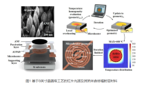
As a core component of nondispersive infrared (NDIR) gas sensors, high-performance MEMS infrared light sources have significant application value in fields such as smart agriculture and environmental monitoring. Existing MEMS infrared light sources generally suffer from bottlenecks such as poor temperature uniformity in the radiation region and high power consumption. Recently, the research team led by Professor Mao Haiyang at the Health Electronics Center of the Institute of Microelectronics proposed a monolithically integrated infrared light source (ANF-IRS) structure based on 8-inch wafer-level technology. By introducing Al nanoparticle-modified nanoforests (ANFs) as a high-emissivity radiating layer, the team significantly improved the device's infrared emission capability at the target wavelength. The research team combined this with iterative optimization of the microheater structure, effectively solving the problem of uneven temperature distribution in traditional light sources, significantly reducing power density while significantly improving operating efficiency. The developed light source has been successfully applied to an integrated NDIR detection system, enabling real-time monitoring of gas concentration fluctuations caused by plant photosynthesis and respiration in a greenhouse environment, providing new low-power hardware support for smart agriculture.​

1768487265532.png
Please, Log in or Register to view URLs content!
 

tokenanalyst

Lieutenant General
Registered Member

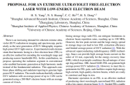
USTC Achieves Breakthrough in Novel Semiconductor Materials


A research team led by Professor Zhang Shuchen from the University of Science and Technology of China (USTC), in collaboration with scientists from Purdue University and ShanghaiTech University, has made a landmark advance in semiconductor technology. For the first time, they successfully created a controllable, atomically flat "mosaic" heterostructure within a two-dimensional ionic soft-lattice material specifically, a halide perovskite using an innovative self-etching approach.

Published online in Nature on January 15, the study overcomes a major challenge in semiconductor fabrication: achieving high-quality lateral (in-plane) heterojunctions in delicate, flexible materials. Traditional methods like photolithography often damage fragile 2D perovskites due to aggressive chemical reactions, limiting device performance and integration.

The team’s breakthrough lies in harnessing internal stress naturally present in growing single crystals. By designing a mild ligand-solvent environment, they triggered selective "self-etching" at specific sites, forming precise square-shaped pores. These were then filled with different semiconductor materials via rapid epitaxial growth, resulting in seamless, atomically flat interfaces across the entire wafer without splicing separate pieces.

“This isn’t just assembling parts it’s guiding a crystal to self-assemble its own functional structure,” said Zhang Shuchen. “We’re paving the way for ultra-thin, densely packed light-emitting pixels that can emit multiple colors on a single chip revolutionizing next-generation displays and optoelectronic devices.”

The work represents the first successful designable fabrication of lateral heterojunctions in 2D ionic semiconductors. It introduces a new paradigm: using internal stress to program crystal evolution, enabling precise control over material structure at the atomic level.​

This achievement opens new pathways for fundamental studies of interface physics and advances the integration of low-dimensional materials into high-performance, miniaturized electronic and photonic devices.

Please, Log in or Register to view URLs content!
 

tokenanalyst

Lieutenant General
Registered Member

Lithography mask project has commenced with an investment of 2 billion yuan!​


The Xingcai Photomask Substrate R&D, Production, and Industrialization Project in Shaoxing’s Hangzhou-Shaoxing Airport Economic Zone has made significant progress. Led by Xingcai Semiconductor Technology (Shaoxing) Co., Ltd., the project aims to produce unpatterned photomask substrates essential components in semiconductor manufacturing that transfer circuit designs onto wafers via photolithography.
1768487994152.png
With a 2-billion-yuan investment and a 40-mu footprint, the facility will eventually produce 60,000 blank photomask substrates annually, including equal shares of binary (BIM) and phase-shift (PSM) types. Products span both mature and advanced processes, supporting logic chips, memory, and power devices.

The project plans a phased rollout—complete pile driving before the Spring Festival, structural topping by July, equipment installation by September, and trial production soon after. Its goal is to establish China’s leading, globally competitive photomask material supply chain, break foreign technological monopolies, and alleviate domestic semiconductor industry bottlenecks. The facility aims to become the most advanced and capable independent domestic manufacturer in this critical field.

Please, Log in or Register to view URLs content!
 

tokenanalyst

Lieutenant General
Registered Member

Smartsens introduces a new 8.3MP high-performance automotive-grade CMOS image sensor​


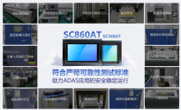
SmartSens (688213) has launched the SC860AT, a high-performance, 8.3MP automotive-grade CMOS image sensor built on its advanced CARSens® - XR Gen 2 Plus platform. Designed for next-generation ADAS and in-cabin vision systems, the SC860AT delivers exceptional imaging performance with key innovations:

1768489246044.png
  • High Frame Rate & Dual Exposure Control: Supports up to 45fps with AB-Exposure™ dual-frame exposure, enabling independent exposure settings for two frames—ideal for handling dynamic scenes like LED traffic lights (frame A: >10ms fixed exposure) and bright conditions (frame B: auto-exposure), eliminating flicker, overexposure, and motion blur.​
  • Superior Image Quality: Features a single-pixel architecture, Lofic HDR® 2.0 + VS four-frame HDR technology, achieving up to 140dB dynamic range with zero motion blur. This ensures clear imaging in extreme lighting conditions both bright (e.g., oncoming headlights) and dark (nighttime or underground parking).​
  • Advanced Technologies: Incorporates SFCPixel® for reduced crosstalk and color inaccuracies, along with LFS (LED Flicker Suppression) technology to deliver flicker-free visuals of traffic lights and vehicle signals critical for reliable ADAS decision-making.​
  • Robust Reliability & Packaging: Uses an upgraded iBGA package, offering superior thermal stability, electrical performance, mechanical durability, and lower failure rates compared to traditional CSP. Passes rigorous reliability tests (temperature cycling, vibration, aging), ensuring long-term safety in automotive applications. Also available in RW and COB packaging for flexible design integration.​
  • Automotive Safety Compliance: Meets both ISO 26262 ASIL-B (functional safety) and ISO 21434 (cybersecurity) standards—essential for safe, secure deployment in ADAS and cabin monitoring systems (OMS), electronic rearview mirrors (E-Mirror), and multi-view cameras.​
  • Cost & Performance Balance: Combines high performance with competitive cost advantages through mature process technology and a stable supply chain, supporting rapid adoption across front-, side-, rear-view, and cabin camera applications.​
"The SC860AT represents a leap forward in automotive imaging delivering high performance, reliability, and cost efficiency. Paired with our 3MP sensors, it supports comprehensive vision solutions for 7V and 11V systems, accelerating the evolution of intelligent driving."

SmartSens plans to continue R&D investment and strategic supply chain collaboration to accelerate innovation from lab to mass production enabling safer, smarter, and more reliable automotive vision systems.

Please, Log in or Register to view URLs content!
 

tokenanalyst

Lieutenant General
Registered Member

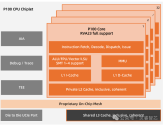
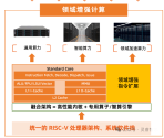
Lingrui Chip Releases the World's First Dynamic 4-Thread Server-Grade High-Performance RISC-V CPU Core P100​


With the deep integration of the Internet of Things and artificial intelligence, we are rapidly entering a ubiquitous intelligent era where computing is everywhere. The form and architecture of computing infrastructure are undergoing profound changes, and computing efficiency and energy efficiency have become key challenges in improving computing power. Converged computing and domain-enhanced computing based on software and hardware collaborative innovation have become the mainstream directions for the development of computing systems. In this process, the open, flexible, and intellectual property-free RISC-V architecture has injected unprecedented vitality and momentum into the computing industry. High-performance, independently controllable RISC-V CPU cores are becoming the core engine driving industrial upgrading and solidifying the foundation of computing power.
1768491077640.png1768491127694.png
Lingrui Chip's groundbreaking P100, the world's first dynamic 4-thread , server-grade , and highest-performance RISC-V CPU core, is a strategic product responding to the call of the times, supporting converged computing and domain-enhanced computing, especially artificial intelligence computing. Through various innovative designs, the P100 successfully fills the gap in domestically produced ultra-high-performance RISC-V cores, marking a significant milestone in China's development of high-value RISC-V products. Simultaneously, based on the P100 core, Lingrui Chip has planned a domain-enhanced processor product roadmap and has initiated related chip product development, aiming to provide strong support for the development of new-quality, new-domain productivity in the RISC-V field, including high-performance, high-reliability server-side enhanced CPUs and AI edge computing chips.

Please, Log in or Register to view URLs content!
 

tokenanalyst

Lieutenant General
Registered Member

Jingzhan Semiconductor Achieves Key Breakthrough in GaN Power Devices​


Recently , Jingzhan Semiconductor has made significant progress in the field of high-voltage gallium nitride (GaN) power devices. The research results, in which Jingzhan Semiconductor played a key role and collaborated with the research groups of Professors Zhang Yuhao and Wang Han at the University of Hong Kong, have been successfully selected for the 2025 IEEE International Electron Devices Meeting (IEDM 2025).

The selected paper reports for the first time an enhanced multi-channel monolithically integrated GaN bidirectional switch, which achieves a 5 kV symmetrical breakdown voltage in both positive and negative polarities, breaking the record for the highest voltage of a monolithic GaN bidirectional device and achieving the best performance indicators among current bidirectional GaN devices .

1768508755492.png

GaN bidirectional power devices are considered to bring revolutionary changes to AI data centers, vehicle charging, photovoltaic and energy storage inverters, and other fields. With the rapid development of next-generation AI energy systems, bidirectional devices have become a core foundation for AC power conversion and new power architectures. However, the voltage of existing GaN bidirectional devices has long been limited to 650V, severely restricting their application in medium- and high-voltage scenarios. Compared to the traditional solution that relies on multiple unidirectional devices connected in reverse series, the advantages of monolithically integrated bidirectional devices will continue to amplify with increasing voltage levels, demonstrating irreplaceable potential in terms of chip area, parasitic parameters, system complexity, and reliability. The realization of this 5 kV monolithic GaN bidirectional device marks a key breakthrough for GaN technology in medium-voltage AC applications.

This device is fabricated on a 6-inch sapphire substrate five-channel GaN epitaxial wafer. The multi-channel structure significantly improves current density and reduces the specific on-resistance to 20 mΩ·cm². Simultaneously, a dual-junction termination extended electric field modulation design is introduced to achieve a high breakdown voltage of 5 kV. Reliability testing shows that under 1.7 kV, 150°C high-temperature reverse bias (HTRB) conditions, the device's on-resistance drift is less than 5%, and the dynamic Ron stability is improved by approximately 30% compared to single-channel devices. Furthermore, it is insensitive to substrate bias changes, demonstrating the intrinsic reliability advantages of the multi-channel GaN structure on the sapphire substrate.

Please, Log in or Register to view URLs content!
 

tokenanalyst

Lieutenant General
Registered Member

RISC-V chip company Advanced Space Technology completes over 600 million yuan Series B financing.​


Chinese RISC-V chip company SpacemiT has raised more than 600 million yuan (approximately US$86 million) in its latest Series B funding round, aiming to accelerate product commercialization and expand its business.

Hangzhou-based Jindie Space announced that Huaxia Hengtian Capital Management Co., Ltd. participated in this Series B financing round. Other participants included the Beijing Artificial Intelligence Industry Investment Fund, an investment institution under the Agricultural Bank of China, Lenovo Group, and Brizan Ventures.

Brizan Ventures led the Series A+ funding round for Advanced Space Technology in January 2025, raising hundreds of millions of RMB. Founded in 2021, Advanced Space Technology is dedicated to designing chips based on the RISC-V architecture, which can be created and customized for free.

Advanced Space Technology (AST) announced that its first chip, K1, has entered mass production, with shipments exceeding 150,000 units. This chip is used in industrial systems, robotics, edge computing, and artificial intelligence (AI) devices.

China is accelerating the research and development of RISC-V and has released plans covering R&D, standards, applications, and global cooperation. Industry participants include Alibaba DAMO Academy, Nuclei Technology, and VeriSilicon Holdings.

Please, Log in or Register to view URLs content!
 
Top