You are using an out of date browser. It may not display this or other websites correctly.
You should upgrade or use an alternative browser.
You should upgrade or use an alternative browser.
Chinese semiconductor thread II
- Thread starter vincent
- Start date
-Tariffs will either add to the pain of US Semiconductor Equipment makers of losing market share in China
- or US Equipment Makers are going to ironically move their remaining production out the US to avoid the "US Import Taxes"
Industry estimates: US tariffs could cost chip equipment makers more than $1 billion a year
U.S. President Donald Trump’s new tariffs could cost U.S. semiconductor equipment makers more than $1 billion a year, according to calculations of the tariff costs discussed last week by lawmakers, administration officials, chip industry executives and officials from international trade group SEMI, two people familiar with the matter said.
The three largest U.S. chip equipment makers - Applied Materials Inc, Lam Research Inc and KLA-Tencor - could each take a hit of about $350 million a year from tariffs, while smaller rivals such as Onto Innovation Corp could also face tens of millions of dollars in extra expenses, the sources said.
The companies make some of the world’s most popular chipmaking equipment, which can require thousands of specialized parts.
Chip equipment makers have lost billions of dollars in revenue following export controls on advanced semiconductor manufacturing equipment implemented by former U.S. President Biden.
The Trump administration has largely suspended reciprocal tariffs announced in April. But in an effort to spur U.S. manufacturing, the administration is considering further tariffs on the chip industry and on Monday launched an investigation into imports from the sector.
The estimated costs discussed in Washington last week include lost revenue, mostly from missed sales of low-end equipment to overseas competitors, and the cost of finding and using alternative suppliers for complex components of chipmaking tools. They also include tariff compliance costs, such as adding staff to handle the complexities of complying with the rules.
Why did they do that? They know they will be fined for exporting those chips.
This report is written off of a filing from a week ago. But right after that on the same day there were other reports that Trump backtracked on it. May be they would just keep the licensing requirement in place and then give a license to Nvidia. For example this one from April 9.
Trump administration backs off Nvidia's 'H20' chip crackdown after Mar-a-Lago dinner
When Nvidia CEO Jensen Huang attended a $1 million-a-head dinner at Mar-a-Lago last week, a chip known as the H20 may have been on his mind.
Following the Mar-a-Lago dinner, the White House reversed course on H20 chips, putting the plan for additional restrictions on hold, according to two sources with knowledge of the plan who were not authorized to speak publicly.
Huawei is making waves with its new AI accelerator and rack scale architecture. Meet China’s newest and most powerful Chinese domestic solution, the CloudMatrix 384 built using the Ascend 910C. This solution competes directly with the GB200 NVL72, and in some metrics is more advanced than Nvidia’s rack scale solution. The engineering advantage is at the system level not just at the chip level, with innovation at the networking, optics, and software layers.
Source: Huawei
The Huawei Ascend chip is not new to SemiAnalysis, but in a , Huawei is pushing the limits of AI system performance. There are trade-offs, but given export controls and lackluster domestic yields, it’s clear that there are further loopholes in the Chinese export controls.
While the Ascend chip can be fabricated at SMIC, we note that this is a global chip that has , , and is fabricated by . We do a deep dive into what is possible for domestic Chinese production what is an aggressive skirting of the export controls, and why the US government needs to focus on these key new areas to limit China’s AI capabilities.
Huawei is a generation behind in chips, but its scale-up solution is arguably a generation ahead of Nvidia and AMD’s current products on the market. So what would be the specifications for Huawei’s CloudMatrix 384 (CM384)?
The CloudMatrix 384 consists of 384 Ascend 910C chips connected through an all-to-all topology. The tradeoff is simple: having five times as many Ascends more than offsets each GPU being only one-third the performance of an Nvidia Blackwell.
Source: SemiAnalysis, Nvidia, Huawei
A full CloudMatrix system can now deliver 300 PFLOPs of dense BF16 compute, almost double that of the GB200 NVL72. With more than 3.6x aggregate memory capacity and 2.1x more memory bandwidth, Huawei and China now have AI system capabilities that can beat Nvidia’s.
What’s more, is the CM384 is uniquely suited to China’s strengths, which is domestic networking production, infrastructure software to prevent network failures, and with further yield improvements, an ability to scale up to even larger domains.
The drawback here is that it takes 3.9x the power of a GB200 NVL72, with 2.3x worse power per FLOP, 1.8x worse power per TB/s memory bandwidth, and 1.1x worse power per TB HBM memory capacity.
The deficiencies in power are relevant but not a limiting factor in China.
China has No Power Constraints, just Silicon Constraints
The common refrain in the West is that , but in China, this is the opposite. The West has spent the last decade shifting a primarily coal-based power infrastructure to greener natural gas and renewable power generation paired with more efficient energy usage on a per capita basis. This is the opposite in China, where rising lifestyles and continued heavy investment mean massive power generation demand.
Most of this has been powered by coal, but China also has the largest install bases of solar, hydro, wind, and now is the leader in deploying nuclear. The United States just maintains the nuclear power deployed in the 1970s. Put simply, upgrading and adding capacity to the US energy grid is a lost muscle, meanwhile in China they have added an entire US grid of capacity since 2011, or approximately the last 10 years.
If you do not have a power constraint because of your relative power abundance, it makes sense to forgo power density and increase scale-up, including optics in the design. The CM384 design considers system-level constraints even outside of the rack, and we believe that it’s not just the relative power availability that constrains China’s AI ambitions. We think that there are multiple ways for continued scaling for Huawei’s solution.
How Many Ascend 910C and CloudMatrix 384 Can China Make?
One common misconception is that Huawei’s 910C is made in China. It is entirely designed there, but China still relies heavily on foreign production. Whether it be HBM from Samsung, wafers from TSMC, or equipment from America, Netherlands, and Japan, there is a big reliance on foreign industry.While SMIC, the largest foundry in China, does have 7nm, the vast majority of Ascend 910B and 910C are made with TSMC’s 7nm. In fact, the US Government, TechInsights, and others have acquired Ascend 910B and 910C and every single one used TSMC dies. Huawei was able to circumvent the sanctions on them against TSMC by purchasing ~$500 million of 7nm wafers through another company, Sophgo.
, only 2x what they profited. It is rumored Huawei continues to receive wafers from TSMC via another 3rd party firm, but we cannot verify this rumor.
Huawei’s HBM Access
Leading edge foreign reliance is part of the equation here, but China is even more reliant on HBM. China is not able to manufacture this reliably with CXMT still a year away from ramping any reasonable volume. Luckily Samsung has come to the rescue, having been the number one supplier of HBM to China through which Huawei has been able to stockpile a total of 13 million HBM stacks which can be used for 1.6 million Ascend 910C packages before any HBM bans.Furthermore, this banned HBM is still being re-exported to China. The HBM export ban is specifically for raw HBM packages. Chips with HBM can still be shipped as long as they don’t exceed the FLOPS regulations. CoAsia Electronics is the sole distributor of HBM for Samsung in Greater China and they have been shipping HBM2E that is to ASIC design service company Faraday who gets SPIL to “package” it alongside of a cheap 16nm logic die.
Faraday then ships this system in package to China, which is technically allowed, but Chinese companies can then recover the HBM by desoldering. We think they employ techniques to make it very easy for the HBM to be extracted from the package, like using very weak low-temperature solder bumps, so when we say it is “packaged,” we mean this in the loosest way possible.
Source: CoAsia Electronics
It is no coincidence that CoAsia’s revenue has exploded since 2025, right after these export controls came into force.
Chinese Domestic Foundry Can Still Ramp
Foreign production is still required, but China’s domestic semiconductor supply chain capability has rapidly improved and is still underestimated. We’ve been consistently sounding the alarm on SMIC and CXMT’s fabrication abilities. Yield and throughput are still issues but the question is what happens longer term with China’s GPU production ramp.Both SMIC and CXMT have received , and they still receive from foreign countries despite sanctions.
Source: SemiAnalysis
SMIC is adding capacity in Shanghai, Shenzhen, and Beijing for advanced node capacity. They will have nearly 50,000 wafers per month of capacity this year, and they continue to expand due to continued access to foreign tools and the lack of effective sanctions and enforcement. If they increase their yield, they can reach serious numbers on Huawei Ascend 910C packages.
While TSMC has provided 2.9 million dies which is enough for 800 thousand Ascend 910B’s and 1.05 million Ascend 910C’s across 2024 and 2025, the SMIC production has the potential to massively grow the capacity if HBM, wafer fabrication tools, tool servicing, and chemicals such as photoresist are not effectively controlled.
CloudMatrix 384 System Architecture
Next let’s dive into the CloudMatrix 384 architecture, scale up networking, scale-out networking, power budget, and cost.A full CloudMatrix system is spread across 16 racks, with each of the 12 compute rack containing 32 GPUs. In the middle of these 16 racks is 4 racks of scale up switches. To bring up world size, Huawei is scaling up across multiple racks and to do that Huawei has had to use optics. Getting to 100s of GPUs in an all-to-all scale up like Huawei is not an easy feat.
Source: SemiAnalysis
Similarities to DGX H100 NVL256 “Ranger”
, but decided to not bring it to production due to it being prohibitively expensive, power hungry, and unreliable due to all the optical transceivers required and the two tiers of network. The CloudMatrix Pod requires an incredible 6,912 400G LPO transceivers for networking, the vast majority of which are for the scaleup network.CloudMatrix384 Scale-Up Topology Estimates
The following section will explain in depth the rack architecture of their scale up NVLink competitor between 384 chips, their scale out networking, power budget break down for the entire system and implications on the massive number of optics and lack of copper cables. We will also discuss cost and the heavy use of LPO transceivers from Huawei.The cess is charged based on a confusing and ambiguous executive order. LA port couldn't collect it because the computers glitched as they were confused by the actual rate of cess.This report is written off of a filing from a week ago. But right after that on the same day there were other reports that Trump backtracked on it. May be they would just keep the licensing requirement in place and then give a license to Nvidia. For example this one from April 9.
Trump administration backs off Nvidia's 'H20' chip crackdown after Mar-a-Lago dinner
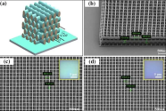
Breaking through the bottleneck! Zhejiang University achieves nanoscale super-resolution laser direct writing technology
Zhejiang University researchers used high-speed laser direct writing to create lines with a spacing of only 100 nanometers on a glass substrate for the first time . The optimized printing method can achieve super-resolution 3D direct laser writing (DLW) of microlenses, photonic crystals , micro-optical devices, metamaterials, etc.

The team emphasizes that an important application of this DLW technology is printing optical waveguide devices for virtual reality or augmented reality displays .
DLW primarily uses a focused laser beam to selectively solidify or polymerize materials with nanometer-scale precision. DLW typically utilizes multiphoton polymerization to polymerize materials in a precise 3D manner.
"Increasing the resolution -- the minimum distance between two adjacent features -- is difficult because the intense laser light causes unnecessary exposure of nearby areas during DLW," said researchers from Zhejiang University. "However, by using a unique dual-beam optical setup and a special photoresist, we were able to overcome this challenge and achieve super-resolution DLW."
Experiments showed that they were able to achieve a record-breaking lateral resolution of 100 nm at a printing speed of 100 μm/s. When using a faster writing speed of 1000 μm/s, a lateral resolution of 120 nm was achieved.
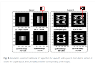
Information theoretical computational lithography based on pattern density statistics.
Abstract
Computational lithography is an important technology to improve the image resolution and fidelity of the optical lithography process. Recently, information theoretical models were introduced to explore the physical limit of image fidelity that can be achieved by different computational lithography methods. However, the existing models were derived based on a simple and idealized assumption of uniform pattern density, thus rendering a loose lower bound on the lithography imaging error. This work improves the accuracy of the information theoretical model by introducing a statistical approach of pattern density. In particular, a density classification rule (DCR) of mask and print image is established based on a number of randomly generated layout samples. The information transfer function between the mask and print image is formulated under the DCR constraint. Then, the optimal information transfer (OIT) and the theoretical limit of lithography image fidelity are derived using a numerical optimization algorithm with mask manufacturing regularization. It has been proved analytically and experimentally that our proposed model provides a much more accurate theoretical limit of lithography image fidelity than the conventional approach.


