Chinese semiconductor thread II

tokenanalyst

Brigadier
Registered Member

China's EDA giant Generali Semiconductor has acquired 100% equity of Ruichengxinwei!​


On April 12, Prologis announced that the company intends to purchase 100% of the equity of Chengdu Ruichengxinwei Technology Co., Ltd. (hereinafter referred to as Ruichengxinwei) and 45.64% of the equity of Naneng Microelectronics (Chengdu) Co., Ltd. (hereinafter referred to as Nanengwei) by issuing shares and paying cash, and raise supporting funds. This transaction is expected to constitute a major asset reorganization and a related transaction, and will not lead to a change in the company's actual controller. The company's stock will resume trading from the opening of the market on April 14, 2025.

Prior to this transaction, Prologix's main products and services included manufacturing EDA, design EDA, semiconductor device characteristic test systems and technology development solutions. The target company is mainly engaged in semiconductor IP design, licensing and related services. Prologix and the target company are both in the integrated circuit design industry, and both parties' businesses are key links in the upstream of the integrated circuit industry chain.

Referring to the development paths of international EDA giants such as Synopsys and Kontronics, the deep collaboration between EDA and IP is the only way for leading EDA companies to develop, and is also an important support for promoting process evolution in the integrated circuit industry and improving the competitiveness of high-end chips.

As the first EDA listed company in China, through this transaction, Prologix will become the first listed company in China with deep collaboration between EDA and semiconductor IP, and can provide comprehensive EDA and IP solutions to dozens of wafer fabs and hundreds of design company customers, while promoting the construction of domestic EDA and IP ecosystems and enhancing the overall competitiveness of the industry. The improvement of EDA product technology level requires long-term collaboration with customer applications, and actual design application cases are an important driving force for the continuous improvement and maturity of EDA products.

Please, Log in or Register to view URLs content!
 

tokenanalyst

Brigadier
Registered Member

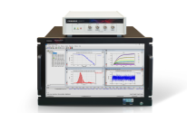
The new generation of semiconductor device characteristics test system FS800 and advanced low-frequency noise test system 9813DXC from ProPlus​


FS800 semiconductor device characteristic test system adopts self-developed test hardware architecture and data bus, with comprehensive functions and flexible configuration. It supports current voltage (IV) test, capacitance voltage (CV) test, fast waveform generation and test, and high-speed time domain signal acquisition. It can complete the automatic test of wafer-level device electrical parameters, parallel test or automatic switching test of array devices in a single desktop device. It can be widely used in new materials and new device research, electrical parameter test, device model data test, reliability test and other fields.


1744641001008.png


As a single complete low-frequency noise test system, 9813DXC supports high-precision noise testing of a wide range of semiconductor device types under various conditions such as 200V high voltage and 100pA ultra-low current. It provides wafer-level noise test accuracy and test bandwidth. The system current noise resolution can reach 10-27 A2 / Hz , and it can adapt to the measurement impedance range of 10Ω-10MΩ. It has a wide range of applications, supporting process quality assessment from mature to advanced processes, device SPICE model development, noise-sensitive integrated circuit design and verification, and other applications.

Please, Log in or Register to view URLs content!
 

tokenanalyst

Brigadier
Registered Member

Tongfu Microelectronics, net profit surges 944% in 2024​


On the evening of April 11, Tongfu Microelectronics released its 2024 annual report. During the reporting period, the company achieved operating income of 23.882 billion yuan, a year-on-year increase of 7.24%; net profit attributable to shareholders of listed companies was 678 million yuan, a year-on-year increase of 299.90%; net profit attributable to the parent company after deducting non-recurring items was 621 million yuan, a year-on-year increase of 944.13%.

In 2024, Tongfu Microelectronics will achieve comprehensive growth in core areas such as SoC, Wi-Fi, PMIC, and display driver. Shipments of mid-to-high-end mobile phone SoCs increased by 46% year-on-year, RF products increased by 70%, and analog devices increased by nearly 40%; product lines such as Bluetooth, MiniLED, and display driver also achieved growth of more than 30%.
Image source: Tongfu Microelectronics

Automotive products performed well. Tongfu Microelectronics expanded its cooperation with leading companies at home and abroad, and its automotive product performance surged by more than 200% year-on-year; in terms of Memory business, the company deepened its collaboration with original manufacturers, and its revenue increased by more than 40% year-on-year; in terms of FCBGA products, it achieved a 52% increase in FC across the board.

In 2024, Tongfu Microelectronics' R&D investment reached 1.533 billion yuan, a year-on-year increase of 31.96%. It has made a number of advances in advanced packaging technology. The industry's smallest SIP device has been mass-produced and the capacitor back-mounting SMT and ball-planting connection operation capabilities have been established; the advanced chip packaging technology based on glass substrate (TGV) has made important progress and successfully passed the phased reliability test. In the field of mature packaging and testing technology, Tongfu Microelectronics continues to promote cost reduction and quality improvement.

As of the end of 2024, Tongfu Microelectronics has accumulated 1,656 domestic and foreign patent applications, of which invention patents account for about 70%; at the same time, Tongfu Microelectronics has successively obtained technology licenses from Fujitsu, Casio, and AMD, enabling the company to quickly enter the high-end packaging and testing field.

It is worth noting that in 2024, the annual turnover of AMD, a major customer of Tongfu Microelectronics, reached a record high of US$25.8 billion. Tongfu Microelectronics is AMD's largest packaging and testing supplier, accounting for more than 80% of its total orders; and AMD business accounts for 50.35% of Tongfu Microelectronics' revenue in 2024.​

Please, Log in or Register to view URLs content!
 

tokenanalyst

Brigadier
Registered Member

Deep learning-based spatiotemporal sequence forecasting of physical fields in tin droplet laser-produced plasma.​

Abstract​

To address the computational challenges in modeling laser produced plasma spatiotemporal evolution, this study pioneers the application of neural operators for two-dimensional radiation hydrodynamics (RHD) simulations in fiber laser produced plasma systems employing liquid tin droplets for extreme ultraviolet lithography (EUVL) sources. Our novel framework enables rapid prediction of multi-physics field evolution by learning the underlying physical operators governing the complex interplay between radiation transport, hydrodynamic motion, and plasma dynamics in EUV light source configurations. Through comparative analysis with Convolutional Long Short-term Memory (ConvLSTM) and Convolutional Neural Operator (CNO) architectures, using over 50,000 spatiotemporal snapshots generated by FLASH software, the multi-variable Fourier Neural Operator (FNO) demonstrates superior performance in all three cases. In the case of single-laser pulse scenarios, it achieves an electron density mean squared error (MSE) of 7.49×10⁻⁵, representing a 53% improvement over ConvLSTM (1.58×10⁻⁴) and a 50% improvement over CNO (1.51×10⁻⁴) in the normalized domain. The FNO exhibits unique zero-shot super-resolution capabilities, reconstructing high-fidelity 96×192 grid solutions from low-resolution 48×96 inputs while maintaining a normalized MSE of 10⁻⁴ relative to ground truth simulations. Demonstrating six-order-of-magnitude acceleration compared to conventional RHD solvers, this approach enables real-time analysis of plasma evolution patterns critical for EUVL source optimization, including tin droplet fragmentation dynamics and extreme ultraviolet emission characteristics. The demonstrated multi-physics modeling capability and memory-efficient super-resolution reconstruction position FNO as a potential transformative tool for next-generation plasma diagnostics and EUVL system monitoring.

Please, Log in or Register to view URLs content!
 

tokenanalyst

Brigadier
Registered Member

The first main equipment of Foshan Qingyi Optoelectronics was successfully moved in and is about to be completed.​


According to the official WeChat account of Shenzhen Qingyi Optoelectronics Co., Ltd., on April 10, the first exposure machine moving-in ceremony was successfully held at the construction site of Foshan Qingyi Optoelectronics High-precision Mask Production Base, marking that the Foshan Qingyi Optoelectronics High-precision Mask Production Base has officially entered the equipment moving, installation and debugging stage.

It is understood that the total investment of Qingyi Optoelectronics in the new production base in Foshan is 3.5 billion yuan. The planning of the base covers the production of high-precision mask plates and high-end semiconductor mask plates. Among them, the total investment of the high-precision mask plate production base construction project is 2 billion yuan, with a planned annual production capacity of 20,000 pieces, which will fill the gap in high-end mask plate production in South China and help the domestic chip industry chain to be independent and controllable.

The company's project team will take the move-in of the first main equipment as an opportunity to fully launch equipment joint debugging and process verification, accelerate the completion acceptance process, strictly control node targets, and ensure that the project is put into trial production as scheduled. According to the plan, Foshan Qingyi Optoelectronics will achieve mass production by the end of 2025. In the future, it will also deploy R&D centers, cooperate with universities and research institutes to tackle the next generation of semiconductor material technology, and inject stronger momentum into the "China Core".

Please, Log in or Register to view URLs content!
 

tokenanalyst

Brigadier
Registered Member

VeriSilicon Unveils a High-Efficiency LCEVC Video Decoder Supporting 8K Ultra HD​


VeriSilicon (688521.SH) today announced the launch of the VC9000D_LCEVC, a next-generation Low Complexity Enhancement Video Coding (LCEVC) video decoding IP. Designed for high-performance and energy-efficient video processing, VC9000D_LCEVC is used in conjunction with VeriSilicon’s VC9000D base video decoder to deliver up to 8K Ultra HD decoding, making it ideal for advanced multimedia applications such as smart TVs, set-top boxes (STBs), and mobile devices.
LCEVC, also known as MPEG-5 Part 2, is the latest standard by the Moving Picture Experts Group (MPEG) and the International Organization for Standardization (ISO). It specifies an enhancement layer which, when combined with a base video encoded with a separate codec, produces an enhanced video stream. The enhancement stream provides new features such as extending the compression capability of the base codec, lowering encoding and decoding complexity, and providing a platform for additional future enhancements. The VC9000D_LCEVC decoder is fully compliant with ISO/IEC 23094-2 (LCEVC) Main Profile, supporting up to Level 4.1. It processes 8/10-bit depth data, accommodates resolutions up to 8192×8192, and employs a frame-by-frame decoding architecture. In addition, it incorporates robust error detection to ensure reliable video playback.
With its high-performance hardware architecture and complete subsystem, VC9000D_LCEVC delivers superior video quality with minimal load on the host CPU. Its integrated Temporal Reference Frame Compression (TRFC) technology significantly reduces system bandwidth usage, while multi-level hierarchical clock gating minimizes dynamic power consumption. It also integrates a post-processor for flexible output format conversion.

Please, Log in or Register to view URLs content!
 
Top