So according to this source mass production cannot begin until the 2030s? This is far behind expected schedules with some people here claiming EUV lines would be ready as soon as 2027.New information:
The EUV prototype machine will likely begin acceptance testing around September (possibly at the national level). The acceptance process will likely extend beyond a month.
The initial production capacity of the current EUV production line is only about 1/8-1/10 that of comparable TSMC lines. Plans aim to increase capacity to half within 1-1.5 years (this refers to throughput capacity, not yield rates). Afterward, it will enter industrial pilot production.
The current phase can be understood as equivalent to the flight testing phase in aircraft development (which typically lasts 4-6 years). This will be followed by small-scale initial production ("Block 1") before achieving true mass production
You are using an out of date browser. It may not display this or other websites correctly.
You should upgrade or use an alternative browser.
You should upgrade or use an alternative browser.
Chinese semiconductor thread II
- Thread starter vincent
- Start date
read the massage again.. the current phase he is talking about, already ongoing. means respective tools and supply chain taking shape.So according to this source mass production cannot begin until the 2030s? This is far behind expected schedules with some people here claiming EUV lines would be ready as soon as 2027.
the initial production capacity is low but by 2027, they will able to achieve volume production with EUV.. then it will enter in industrial production as fully adapted by the industry.
If any chinese company still buy Nvidia and AMD chips after this revelation they deserve to have their models poisoned and go bankrupt
Nothing in the article says the tracking is part of the chips themselves. It says “embed in shipments”, which could be as simple as them sticking Apple AirTags in the boxes or shipping crates.
Which is far more likely because it allows tracking of the actual path of the shipments, if tracking was in the gpu silicon, no way to track who the resellers are unless they plug the servers in and power on the gpu at each stop of the route
a chip can be put in-between the pcb layer and an antenna also put in there.Nothing in the article says the tracking is part of the chips themselves. It says “embed in shipments”, which could be as simple as them sticking Apple AirTags in the boxes or shipping crates.
Which is far more likely because it allows tracking of the actual path of the shipments, if tracking was in the gpu silicon, no way to track who the resellers are unless they plug the servers in and power on the gpu at each stop of the route
Literally impossible. The chip already produces so much heat that is has to be liquid cooled. Air colling has been phased out.a chip can be put in-between the pcb layer and an antenna also put in there.
The largest single-site CVD artificial diamond production base in China
A delegation themed "Counterpart Aid to Xinjiang: A Tide of Tianshan" visited Carbon Core Materials (Xinjiang) Technology Co., Ltd. in the Shache County Industrial Park. This project, funded by Shanghai Pudong Development Bank, has become China's largest single-site chemical vapor deposition (CVD) artificial diamond production base. The initial batch of 678 cultured diamond production lines has been put into operation, generating an annual output value exceeding 1 billion yuan, filling a gap in southern Xinjiang's high-end new materials industry.
Empowered by the Pudong aid team's technical expertise, the company has introduced world-leading microwave plasma chemical vapor deposition (MPCVD) technology, achieving product purity of 99.999%. This technology is widely used in fields such as semiconductors and aerospace, and has become a core supplier to leading companies such as Huawei and SMIC. Pudong has also partnered with research institutions such as Shanghai Jiao Tong University to promote the localization of MPCVD equipment, reducing production costs by 40% and increasing the yield rate to 98%.
The project also led to the construction of five related production lines, including large-scale industrial refrigeration and gas purification, forming a diamond industry cluster with an annual output value of approximately 3 billion yuan; through the targeted training of 300 technical workers, it achieved "high-tech employment at home" with an average monthly income of 8,000 yuan for employees.
The second phase of the plan will expand to 1,500 to 3,000 production lines, reaching an annual output of 500,000 carats upon reaching full capacity, projecting a 15% share of the global cultured diamond market. In 2024, the company was designated a "National High-Tech Enterprise," becoming a model for targeted aid to Xinjiang through "scientific and technological innovation." It is expected to drive the coordinated development of precision machining, equipment manufacturing, and other industries in southern Xinjiang, contributing to the establishment of a new materials industry chain worth hundreds of billions of yuan.
Xinyuan Micro (KingSemi) - Striving to Become a Pioneer in Liaoning's Integrated Circuit Equipment Industry
Xinyuanwei has blazed a trail on the road of domestic substitution and overcome numerous difficulties and obstacles:
- First, the coating and developing equipment itself is incredibly complex. The most advanced coating and developing machines have over 150 units and more than 10 robotic arms, performing tens of thousands of electromechanical movements per hour. The technical complexity of coating is like laying the floor on a football field; the height difference must be controlled to within the width of a human hair.
- Secondly, the photoresist coating and developing machine must be connected to the most expensive and important lithography machine on the chip production line. Zong Runfu said: "Online verification is difficult, but more importantly, we must not drag down the lithography machine. We must have high requirements for product production capacity, yield rate, and reliability
- Third, Japanese equipment manufacturers started early and have a deep foundation, resulting in a high degree of monopoly in the domestic market, with a monopoly rate exceeding 90%. As R&D progresses and product iterations break through, Xinyuan Micro will further promote the process of domestic substitution.
Xinyuanwei's front-end equipment has covered all process nodes above 28 nanometers, covering more than 90% of China's semiconductor mature processes. Among them, the front-end physical cleaning equipment has reached the international advanced level and successfully achieved domestic substitution; the front-end chemical cleaning equipment focuses on advanced processes and targets the long-term monopoly of foreign countries. Xinyuanwei has become the first domestic company to pass the high-temperature sulfuric acid cleaning process verification and obtain repeat orders. In the field of back-end advanced packaging, Xinyuanwei, as a complete set of process equipment provider, has a product market share of more than 50%, becoming the main mass production equipment supplier for clients. At the same time, it continues to deploy emerging fields such as 2.5D and 3D packaging to develop new growth points.

Based in Liaoning and Shenyang, Xinyuan Microelectronics is committed to independent research and development, with R&D expenses remaining above 10% of operating revenue for many consecutive years. In 2024, its R&D investment reached 297 million yuan, a year-on-year increase of nearly 50%. These technological breakthroughs are poised to translate into substantial market success.

Based in Liaoning and Shenyang, Xinyuan Microelectronics is committed to independent research and development, with R&D expenses remaining above 10% of operating revenue for many consecutive years. In 2024, its R&D investment reached 297 million yuan, a year-on-year increase of nearly 50%. These technological breakthroughs are poised to translate into substantial market success.
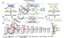
Physics-informed Unsupervised Neural Network for Parametric Analysis and Reconstruction via Scatterometry Evaluation (PUNN-PARSE) of Grating Structures on Extreme Ultra-Violet Collector Mirror
Abstract
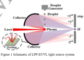
Effective metrology of collector grating structures is crucial for ensuring high spectral purity in extreme ultraviolet lithography (EUVL) light sources. In this paper, we propose a physics-informed unsupervised neural network for parametric analysis and reconstruction via scatterometry evaluation (PUNN-PARSE) of EUVL collector gratings. PUNN-PARSE combines scalar diffraction theory constraints with unsupervised neural networks to directly reconstruct key dimensional parameters from reflectance spectra, without the need for off-line model training or extensive dataset preparation. Under a signal-to-noise ratio of 400:1, the proposed method achieves remarkably low relative errors of 0.218% for height and 0.620% for top angle of deformed trapezoidal gratings, which is sufficient for the measurement requirements for EUV collector gratings. What’s more, the relative standard uncertainties are as low as 0.00376% and 0.0178% for the two parameters, respectively, indicating high data consistency and confidence in the reconstruction results. In addition, the consumption time of PUNN-PARSE is about 10 times faster than conventional methods for inline reconstruction. In a summary, PUNN-PARSE not only enhances the accuracy and speed of reconstruction, but also maintains physical interpretability, making it promising for the inline measurement of gratings’ dimensional


The Institute of Semiconductors and others have made important progress in the quantitative prediction of angle-resolved polarized Raman spectroscopy of anisotropic layered materials
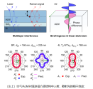
The Institute of Semiconductors research team led by Tan Pingheng has developed a theoretical framework for quantitatively predicting angle-resolved polarized Raman spectroscopy (ARPR) intensities in anisotropic layered materials (ALMs). Their approach addresses a decade-long challenge: explaining why ARPR intensity in ALMs (e.g., black phosphorus, Td-WTe₂) varies with flake thickness and excitation wavelength—a phenomenon previously unresolvable despite studies on birefringence, linear dichroism, and substrate effects.
The team introduced two key tensors:
Intrinsic Raman tensor: An intrinsic property of ALMs reflecting atomic displacement fields during phonon scattering (independent of thickness or substrate).
Effective Raman tensor: Accounts for polarization field modulation in air/ALM/substrate structures and external parameters.
Using BP and four-layer Td-WTe₂ thin films, they measured complex refractive indices along crystal directions and derived R int matrix elements at wavelengths of 633 nm, 532 nm, and 488 nm. This enables quantitative ARPR predictions for ALM flakes of varying thicknesses on arbitrary substrates without fitting parameters. The framework applies to both monolayer/bulk ALMs and non-resonant excitations.
