Chinese semiconductor thread II

tokenanalyst

Brigadier
Registered Member

Simulation study of high-resolution imaging of extreme ultraviolet masks using synchrotron radiation at wavelengths.​


Abstract
Background

Extreme ultraviolet (EUV) lithography is a critical technology for advanced semiconductor manufacturing that requires nearly defect-free EUV masks, necessitating high-resolution actinic (at-wavelength) imaging analysis for mask defect inspection.
Purpose
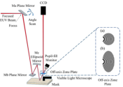
This study aims to explore the potential for achieving higher resolution in actinic mask review by developing an elliptical zone plate design with anisotropic numerical aperture.
Methods
First, a simulation platform was established based on the EUV light generated by undulator equipment at the Shanghai Synchrotron Radiation Facility (SSRF). Second, simulations based on partial coherent light imaging model were performed to evaluate the imaging performance of three different collimator configurations under Fourier-synthesis illumination conditions. Finally, an elliptical off-axis zone plate with anisotropic numerical aperture was designed and optimized through systematic computational studies.
Results
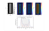
The simulation results demonstrate that the elliptical zone plate design achieves a numerical aperture of 4×NA=1.15 in the horizontal direction, significantly higher than the conventional circular zone plate's 4×NA=0.625. Under extreme dipole illumination conditions, a theoretical resolution of 12 nm half-pitch in the horizontal direction is achieved while maintaining 22 nm resolution in the vertical direction. The anisotropic design effectively overcame the reflectivity limitations of multilayer mirrors at large incident angles (<19°).
Conclusions
The proposed elliptical zone plate design with anisotropic numerical aperture in this study improves the resolution limit by 45.5% compared to conventional circular designs, achieving a 12 nm half-pitch resolution that surpasses the current international benchmark of 22 nm. This advancement provides a promising pathway for next-generation high-resolution EUV mask defect review systems.
1744838627179.png1744838651007.png

Please, Log in or Register to view URLs content!
 

tokenanalyst

Brigadier
Registered Member

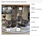
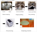
Research on the Trajectory and Relative Speed of a Single-Sided Chemical Mechanical Polishing Machine.​

Abstract​

This study establishes a bidirectional kinematic analysis framework for single-sided chemical mechanical polishing systems through innovative coordinate transformation synergies (rotational and translational). To address three critical gaps in existing research, interaction dynamics for both pad–wafer and abrasive–wafer interfaces are systematically derived via 5-inch silicon wafers. Key advancements include (1) the development of closed-form trajectory equations for resolving multibody tribological interactions, (2) vector-based relative velocity quantification with 17 × 17 grid 3D visualization, and (3) first-principle parametric mapping of velocity nonuniformity (NUV = 0–0.42) across 0–80 rpm operational regimes. Numerical simulations reveal two fundamental regimes: near-unity rotational speed ratios (ωP/ωC = [0.95, 1) and (1, 1.05]) generate optimal spiral trajectories that achieve 95% surface coverage, whereas integer multiples produce stable relative velocities (1.75 m/s at 60 rpm). Experimental validation demonstrated 0.3 μm/min removal rates with <1 μm nonuniformity under optimized conditions, which was attributable to velocity stabilization effects. The methodology exhibits inherent extensibility to high-speed operations (>80 rpm) and alternative polishing configurations through coordinate transformation adaptability. This work provides a systematic derivation protocol for abrasive trajectory analysis, a visualization paradigm for velocity optimization, and quantitative guidelines for precision process control—advancing beyond current empirical approaches in surface finishing technology.​

1744840354054.png1744840383959.png

Please, Log in or Register to view URLs content!
 

tokenanalyst

Brigadier
Registered Member

Driven by technological innovation and global layout, Zhongke Xinyuan leads the new trend of semiconductor thermoelectric temperature control​


In the field of semiconductor manufacturing, temperature control equipment is a key link to ensure process accuracy and product quality. In recent years, as the semiconductor industry has accelerated its transfer to the Chinese market, a number of suppliers focusing on temperature control equipment have emerged in China. Among them, Anhui Zhongke Xinyuan Semiconductor Technology Co., Ltd. (hereinafter referred to as "Zhongke Xinyuan") has gradually become a leader in the industry with its technological innovation and product iteration in the field of thermoelectric semiconductor temperature control systems. At the SEMICON CHINA 2025 exhibition, Jiwei.com had the honor of interviewing Xiong Yi, CEO of Zhongke Xinyuan, and had an in-depth exchange on topics such as the company's product advantages and global market layout.

High-precision temperature control: the "invisible hero" of semiconductor manufacturing
Compared with traditional compression and heat exchanger temperature control equipment, thermoelectric semiconductor temperature control equipment has higher accuracy and flexibility, and can better meet the high-precision control needs in the semiconductor manufacturing process. According to industry experts, thermoelectric temperature control equipment is expected to become the fastest growing type of semiconductor temperature control equipment in the next few years.

Zhongke Xinyuan was established in November 2017, focusing on the research and development of thermoelectric temperature control system products in the field of semiconductor applications. The company launched the Z-3000/Z-6000 and ZMO-500 series direct coolers in the second year after its establishment. So far, Zhongke Xinyuan has formed a thermoelectric temperature control product matrix covering the three major fields of semiconductors, 5G communications, and automotive, and has been favored and repurchased by many domestic and foreign customers.

Zhongke Xinyuan's products are characterized by high integration, high performance, low cost, low power consumption, and easy installation. Taking the Z-6000 semiconductor direct cooling machine as an example, the equipment adopts a highly integrated design, has more convenient troubleshooting and whole machine replacement technology, and is mainly suitable for etching (Etch), chemical vapor deposition (CVD) and physical vapor deposition (PVD) process processes in semiconductor wafer factories.
"Z-6000 is not only fast-response, green and environmentally friendly (no Freon, no noise), but also has high precision (temperature control accuracy ±0.1℃) and high reliability (MTBF>5) and other characteristics." Xiong Yi, founder and CEO of Zhongke Xinyuan, said in an interview, "In addition, Z-6000 is the smallest refrigerator on the market, with significant power consumption advantages, saving an average of about 80% energy compared to traditional compressor temperature control systems."

According to Xiong Yi, using the Z-6000 semiconductor direct cooling machine instead of traditional solutions can save customers an average of about RMB 35,000 in electricity bills each year. The cost saved in 2 to 2.5 years is enough to buy a new direct cooling machine.


Please, Log in or Register to view URLs content!
 

tokenanalyst

Brigadier
Registered Member

Reducing dose sensitivity in high-numerical-aperture extreme ultraviolet lithography using an innovative source optimization method.​

Abstract​


Errors such as illumination non-uniformity and system drift during scanning can lead to unpredictable dose non-uniformity and degrade the imaging performance across the wafer. This paper proposes a novel, to our knowledge, source optimization (SO) method for high-numerical-aperture extreme ultraviolet lithography (high-NA EUVL) system. This method establishes a dose sensitivity function and integrates it into the cost function of the SO process. It aims at reducing the influence of dose variation on the critical dimension error (CDE) in the EUVL system and increasing the exposure latitude (EL). Simulation results demonstrate that this method significantly improves the stability of imaging performance in case of dose non-uniformity. Additionally, it extends the process window (PW).

Please, Log in or Register to view URLs content!
 

tokenanalyst

Brigadier
Registered Member

BIWIN exhibits domestically developed power eMMC to help accelerate the implementation of new power systems​


China Electrical Instrument Industry Development Conference and Exhibition 2025 opened in Chongqing. BIWIN Storage demonstrated its highly reliable and highly stable full-scenario power storage solution to help customers complete the production and implementation of new power system products.
Genuinely made in China, fully self-developed eMMC for power generation

Power customized firmware, stable and long-lasting

The power industry faces harsh environmental challenges such as extreme temperature differences and electromagnetic interference all year round. eMMC, which features integrated design, stable performance, low power consumption, and vibration resistance, is widely used in scenarios such as data collectors, protection devices, concentrators, and fusion terminals that have strict requirements on data integrity and security, ensuring the long-term reliable operation of equipment.
1727457727813.8296.png

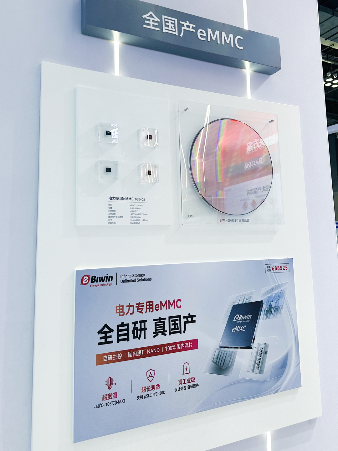
At this exhibition, BIWIN Storage exhibited its 100% domestically produced eMMC specifically for power generation for the first time . The product is equipped with BIWIN's self-developed main control and domestically produced NAND . The entire process from chip design to wafer manufacturing is localized, and the independent and controllable product meets the key demands of the power industry for data security.
BIWIN has taken the right approach in product definition, software and hardware algorithms, testing processes , and manufacturing to ensure that the product is highly compatible with the power industry specifications. The product covers 8GB~128GB capacity , supports a wide operating temperature range of -40℃~105°C , has a P/E erase and write count of >30,000 , and has undergone multiple stability tests and repeated reliability verifications, demonstrating excellent durability and environmental adaptability.
This product uses BIWIN's self-developed firmware algorithm , integrating innovative technologies such as low- power design, power-off protection, wide temperature adaptation, enhanced data protection, and pSLC firmware mode to ensure zero data loss and zero storage interruption in unexpected scenarios such as unexpected power outages and severe weather, thereby maximizing the product life cycle. In view of the "high-frequency small data stream" characteristics of power equipment, BIWIN's self-developed main control deeply optimizes the compatibility between the protocol layer and the power equipment firmware, reduces data transmission delays, ensures the real-time writing of current fluctuation records and fault logs, and avoids the omission of key data.
R&D, packaging and testing are integrated to create a "family bucket" of industrial-grade products

Please, Log in or Register to view URLs content!
 

tokenanalyst

Brigadier
Registered Member

Zhilun Ultrapure completed tens of millions of yuan in A+ round of financing, focusing on the localization of semiconductor materials​


According to Zhilun New Materials' WeChat account, recently, Zhilun Ultrapure, a developer and manufacturer of ultra-high purity electronic-grade epoxy resins, successfully completed a multi-million-yuan A+ round of financing. This round of investment was jointly injected by Star Capital and several strategic investors. The funds raised in this round will be used to build a market ecosystem, deepen customer value, and plan forward-looking industry layout.
Zhilun New Materials Technology (Xi'an) Co., Ltd., founded in May 2022, is a national high-tech enterprise integrating "R&D + production + sales". It focuses on the field of ultra-high purity, low-chlorine electronic-grade epoxy resins and is committed to tailor-making high-standard epoxy high-purity electronic special materials, customized epoxy resins and integrated product solutions for customers in the semiconductor, composite materials, new energy and other industries.
The representative of the investor said: "We highly recognize Zhilun New Materials' breakthrough capabilities in key links of the industry. Its dual-wheel drive model of 'technology research and development + scenario implementation' is reshaping the competitive landscape of the semiconductor materials market. We look forward to opening up a broader value space through strategic collaboration."

Please, Log in or Register to view URLs content!
 

tokenanalyst

Brigadier
Registered Member

Tongguang Technology invested 390 million yuan to produce 70,000 pieces of silicon carbide single crystal substrates annually​


Recently, the National Construction Project Environmental Information Disclosure Platform released the "Announcement on the Completion of the Environmental Protection Acceptance of the Hebei Tongguang Technology Development Co., Ltd. Project with an Annual Production of 70,000 Pieces of Silicon Carbide Single Crystal Substrates". The total investment of the project is 388.635 million yuan, and the environmental protection investment is 3.9 million yuan, accounting for 1.00% of the investment. According to the information, Hebei Tongguang Technology Development Co., Ltd. was established in April 2020 and is located in Hebei Laiyuan Economic Development Zone, Laiyuan County, Baoding City. It is an important subsidiary of Hebei Tongguang Semiconductor Co., Ltd.

Tongguang Semiconductor is a third-generation semiconductor company that is supported by Hebei Province. It focuses on the research and development and production of silicon carbide (SiC) single crystal substrates. Its products are widely used in new energy vehicles, 5G communications, smart grids, etc. Relying on the technical team of the Chinese Academy of Sciences, the company has broken the monopoly of foreign technology and has built a domestically leading SiC mass production line. Its customers cover leading companies, helping China's semiconductor industry chain to be independently controllable.

Please, Log in or Register to view URLs content!
 

tokenanalyst

Brigadier
Registered Member

Critical dimension scanning electron microscope image processing method and electronic equipment​

Institute of Semiconductors of Guangdong Academy of Sciences​

Abstract​

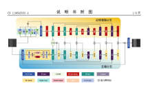
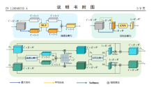
The present invention discloses a critical dimension scanning electron microscope image processing method and electronic device, the method comprises using a pre-trained image processing model to process an input image to obtain an optimized image; the pre-trained image processing model comprises a denoising branch and an edge enhancement branch, both branches are based on a U-Net network architecture, the denoising branch comprises a first encoder module and a first decoder module connected in sequence, the first encoder module and the first decoder module both use an SC block module to extract local and global features of the image; the edge enhancement branch comprises an edge information extraction module, a second encoder module and a second decoder module connected in sequence; and also comprises a feature fusion module for fusing the outputs of the first encoder module and the second encoder module at various levels as inputs of the first encoder module at various levels. Compared with the traditional image denoising algorithm, the algorithm solves the edge blurring problem caused by excessive image smoothing while denoising.

1744901131417.png
1744901146759.png
 

tokenanalyst

Brigadier
Registered Member
Ultrapure Nitrous oxide for lithography machine cleaning

Nitrous oxide double-tower purification process​

CN 119612460 A
Zhejiang Jinhua Air Separation Equipment Co Ltd

Abstract​

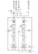
The invention discloses a nitrous oxide double-tower purification process, which relates to the technical field of nitrous oxide purification and comprises the following steps: s1: raw material preparation, namely introducing nitrous oxide raw material into a filtering device to filter out solid impurities, so as to obtain raw material liquid; s2: the method comprises the steps of low-boiling separation, conveying raw material liquid into a first rectifying tower from a feed pipe through a compressor, and separating impurities lower than the boiling point of nitrous oxide in the primary separation raw liquid to obtain primary separation raw material liquid; s3: high-boiling separation, namely conveying primary separation raw liquid into a second rectifying tower from a first rectifying tower, and separating impurities higher than the boiling point of nitrous oxide in the primary separation raw liquid to obtain nitrous oxide liquid; according to the invention, by replacing the adsorption tower with the rectifying tower, the replacement and maintenance cost of the adsorbent is reduced, the equipment complexity of the nitrous oxide purification system is greatly reduced, and the nitrous oxide raw material and the final product is both liquid, so that the nitrous oxide purification system is convenient to store and transport.​

1744901599467.png
 
Top