1. High-speed 3D stacked GaN/SiC cascode power device with superior switching speed control capability
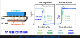
For many years, the low MOS channel mobility ( < 40 cm 2 /V · s ) of commercial SiC MOSFETs has been a bottleneck problem that restricts wide bandgap SiC materials from fully releasing their performance. The GaN/SiC hybrid cascode device proposed by Professor Chen Jing's research group replaces the low-mobility MOS channel of SiC MOSFET with a GaN - based 2DEG channel, greatly improving the channel mobility to around 2000 cm 2 /V · s . In order to give full play to the switching performance of GaN/SiC cascode devices, the team developed a 3D stacked packaging solution for the device, effectively solving the long-standing parasitic inductance bottleneck of sealed devices. Compared with the latest generation of wide bandgap semiconductor 1.2 kV high-power commercial devices, the switching speed of the new device has been significantly improved.
For many years, the low MOS channel mobility ( < 40 cm 2 /V · s ) of commercial SiC MOSFETs has been a bottleneck problem that restricts wide bandgap SiC materials from fully releasing their performance. The GaN/SiC hybrid cascode device proposed by Professor Chen Jing's research group replaces the low-mobility MOS channel of SiC MOSFET with a GaN - based 2DEG channel, greatly improving the channel mobility to around 2000 cm 2 /V · s . In order to give full play to the switching performance of GaN/SiC cascode devices, the team developed a 3D stacked packaging solution for the device, effectively solving the long-standing parasitic inductance bottleneck of sealed devices. Compared with the latest generation of wide bandgap semiconductor 1.2 kV high-power commercial devices, the switching speed of the new device has been significantly improved.
2. All-GaN-based semiconductor gate enhancement HEMT for gate high voltage protection and optical-electrical synchronous drive
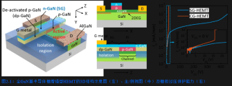
In recent years, p -GaN gate enhancement mode GaN- based power HEMT has achieved rapid development and initial commercialization, but due to the lack of intrinsic gate overvoltage protection structure, the device is troubled by low gate withstand voltage capability and safe gate voltage limit during use. In response to this bottleneck, Professor Chen Jing's research group proposed to use N- type doped GaN cap layer as semiconductor gate to replace the traditional metal gate to construct n-GaN/p-GaN/AlGaN/GaN enhancement mode HEMT . The specific structure is shown in Figure 2-1 , where the n-GaN above the active area channel is the intrinsic gate ( IG ), and the external gate ( XG ) outside the active area is connected to the gate metal to provide gate voltage.
In recent years, p -GaN gate enhancement mode GaN- based power HEMT has achieved rapid development and initial commercialization, but due to the lack of intrinsic gate overvoltage protection structure, the device is troubled by low gate withstand voltage capability and safe gate voltage limit during use. In response to this bottleneck, Professor Chen Jing's research group proposed to use N- type doped GaN cap layer as semiconductor gate to replace the traditional metal gate to construct n-GaN/p-GaN/AlGaN/GaN enhancement mode HEMT . The specific structure is shown in Figure 2-1 , where the n-GaN above the active area channel is the intrinsic gate ( IG ), and the external gate ( XG ) outside the active area is connected to the gate metal to provide gate voltage.
3. Wide-bandgap semiconductor reconfigurable neural transistor for reservoir computing
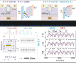
Jing's research group proposed a reconfigurable transistor based on gallium nitride (Figure 3-1 ). The device is based on the p-GaN/AlGaN/GaN platform, uses p- type gallium nitride as the channel material, and combines different gate structure designs to form volatile and non-volatile memory devices, which serve as the reserve layer and readout layer in the reserve pool calculation, respectively. Among them, the volatile device is based on the gate structure of top gate / dielectric / floating gate / semiconductor / back gate, uses the floating gate as the medium for short-term charge storage, and uses the double gate structure to adjust the nonlinear input and output response and short-term memory retention time of the device, respectively, to achieve a reconfigurable physical reserve pool. The non-volatile device is based on the gate structure of top gate / dielectric / semiconductor / back gate, uses the deep energy level trap state of the dielectric / semiconductor interface as the medium for long-term charge storage, and uses electron and hole injection to achieve fast weight update, multi-state storage and high durability. Using this reconfigurable transistor, a highly adaptable reserve pool computing system was further constructed to achieve chaotic time series prediction on different time scales
