Chinese semiconductor thread II

tokenanalyst

Brigadier
Registered Member

Han's Laser won the bid for BOE's 8.6-generation line project again​


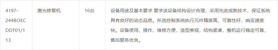
Shenzhen Han's Semiconductor Equipment Technology Co., Ltd. (hereinafter referred to as Han's Semiconductor), a wholly-owned subsidiary of Han's Laser, won the bid for BOE's 8.6th-generation AMOLED production line project, with the project number 4197-244BOECDDT01/113 . After checking, it was found that BOE bid for 16 laser repair machines in this project.

MBXY-CR-47cc595e8525256033be548f1b04d14d.png

After checking, BOE issued the "Announcement on Investing in the Construction of BOE's 8.6th Generation AMOLED Production Line Project" on November 28, 2023. The total investment of the project is 63 billion yuan.

In AMOLED panel manufacturing, laser repair machines are mainly used to repair point defects in the CELL segment of flexible screens, with a focus on precise repair of bright spot defects to restore them to normal display or darkened state. The equipment uses a laser beam focused on the defect position of the screen through an optical system to complete non-contact precision repair. This technology has the characteristics of high precision and non-contact, avoiding secondary damage to the screen, while improving repair efficiency and reducing maintenance costs. In view of the characteristics of flexible screens, the equipment uses a special adsorption structure to ensure that the operation process is damage-free, and integrates an automatic detection system that can accurately identify and repair various defects including micro bright spots.

Please, Log in or Register to view URLs content!
 

OptimusLion

Junior Member
Registered Member
Shanghai Xinwei Semiconductor Co., Ltd.'s patent for "Epitaxial structure of vertical cavity surface emitting laser and its verification method" has been announced. The application publication date is December 27, 2024, and the application publication number is CN119209203A.


1207339515565.3025.png

Please, Log in or Register to view URLs content!
 

OptimusLion

Junior Member
Registered Member
With a total investment of 1 billion yuan, the first production line of the FC-BGA high-end IC packaging substrate project of Aoxin Semiconductor was opened

According to Huangjing news, on February 11, the first production line of Suzhou Taicang City's key project Aoxin Semiconductor FC-BGA high-end IC packaging substrate project was opened. The project is located in Huangjing Town and is a provincial private key project in 2025. The project covers an area of 45 acres and a construction area of 27,000 square meters. The total planned investment is 1 billion yuan to build a high-end IC substrate carrier production line from inner layer to packaging. Since the groundbreaking in May 2023, after nearly two years of intensive construction, the project has successfully completed civil engineering and plant decoration, and equipment has also been put into place. Now the first production line is officially opened and enters a new production stage.

Please, Log in or Register to view URLs content!
 

tokenanalyst

Brigadier
Registered Member

Diamond material company Xinfeng Technology completes a new round of financing, led by Zhongke Chuangxing​


Hunan Xinfeng Technology Co., Ltd. (hereinafter referred to as Xinfeng Technology), a leading domestic company in the innovation and application of diamond functional materials, completed a new round of strategic financing. This round of financing was led by Zhongke Chuangxing, with an investment amount of tens of millions of yuan. This financing will help Xinfeng Technology enter a comprehensive acceleration stage in the layout of industrial research and development in multiple fields such as electrochemistry, thermal science, and optics, the construction of intelligent industrial bases, and the development of new product lines.

Xinfeng Technology is a technology platform enterprise that started with the research and development and production of diamond functional materials. Since its establishment in 1999, the company has a 32-year technical accumulation team and more than 140 independent patent technologies. The company cooperates with many central enterprises, state-owned enterprises, and listed companies such as China Aerospace, PetroChina, Sinopec, CNNC, CGN, Baowu Water Group, and CATL, and has exported related technology products to many countries including the United Kingdom, Germany, the United States, Japan, South Korea, India, and Italy.

Xinfeng Technology has achieved leading results in the field of electrochemical applications, and its products have formed a complete product system. The company is actively deepening its electrochemical application field and rapidly strengthening its scientific research layout in the fields of thermal, optical and semiconductor applications.​


Please, Log in or Register to view URLs content!
 

tokenanalyst

Brigadier
Registered Member

Xiyuan Electronics' high-end semiconductor packaging and testing project has invested 1.2 billion yuan, and the main part has been completed and is expected to be put into production in the first half of the year​

Xiyuan Electronics' high-end semiconductor packaging and testing project is 1.2 billion yuan, with an additional land area of 27.6 acres. The annual production capacity is designed to be about 2.1 billion LGA/FCLGA devices and about 900 million OFN/DFN/SO/MEMS devices. After the project is completed and reaches full production, it is expected to achieve annual sales of 1.5 billion yuan and comprehensive tax revenue of 50 million yuan.

On April 10, 2024, the foundation of Xiyuan Electronics' high-end semiconductor packaging and testing project was laid. According to the news from Juli Donggang at the time, Baikejing Semiconductor Technology (Suzhou) Co., Ltd., as the main investor of the project, is a manufacturing enterprise integrating semiconductor wafer thinning, cutting, core picking and testing. The high-end semiconductor packaging and testing project of Xiyuan Electronic Technology (Wuxi) Co., Ltd. occupies 27.58 acres of land, with a construction area of 36,000 square meters and 2 new factory buildings. The company will purchase about 400 advanced packaging and testing equipment such as grinding and lamination, physical cutting, laser cutting, solid crystal, wafer bonding, plasma cleaning, etc., to create a first-class domestic packaging and testing factory. The products mainly serve domestic first-line integrated circuit design and chip manufacturers. After full production, it is expected to increase the packaging and testing capacity by 288 million pieces.

Please, Log in or Register to view URLs content!
 

OptimusLion

Junior Member
Registered Member
The Chinese Academy of Sciences has made a breakthrough in photonic chip technology and used the "building blocks" method to build a heterogeneous integrated quantum light source on a silicon carbide chip

The research team adopted a "building blocks" hybrid integration strategy to heterogeneously integrate III-V semiconductor quantum dot light sources with CMOS-compatible silicon carbide (4H-SiC) photonic chips to build a new hybrid microring resonant cavity

001ZzMwgly1hyqawaurs2j60n00o2qky02.jpg


001ZzMwgly1hyqawb0orxj60go08241q02.jpg

Please, Log in or Register to view URLs content!
 

tokenanalyst

Brigadier
Registered Member

Domestic semiconductor measurement manufacturers received tens of millions of yuan in financing!​

Corerate Intelligent Technology (Suzhou) Co., Ltd. announced the completion of a B round of financing of tens of millions of yuan. Investors in this round of financing include Longding Investment, Yuanhe Puhua, Changsha Guokong Capital, Changlei Capital, etc. The funds will be mainly used for the research and development of new generation AI detection technology, global market layout and high-end talent introduction to further consolidate its core competitiveness in the field of semiconductor manufacturing.

As a service provider of yield management and localization software replacement in the field of domestic chip manufacturing, Core Rate Intelligence has been committed to providing first-class AI products and solutions focused on yield for the Chinese semiconductor industry by accelerating AI smart manufacturing since its establishment in 2006. The company has developed and launched dozens of AI tool software for yield analysis and process optimization, including AI YMS, AI ADC, AI DMS, AI RMS, AI MVA, AI SSA, MTA, AI Metrology, Dynamic Sampling, Virtual Metrology, TEM measurement, HLA, etc., and has successfully introduced and applied them in more than a dozen mass production lines, including SMIC, SMIC Shaoxing SMIC, Huahong Grace, Huahong Wuxi, GalaxyCore, and Jetta Semiconductor.
The technical advantage of ChipSeek lies in its focus on process control of the production process of AI product service production lines.

By combining with production line production machines and process nodes, it has accumulated a large amount of process know-how and built its own industry big model ChipSeek. The commercial mass production of ChipSeek marks the entry of domestic semiconductor AI industrial software into the cognitive intelligence stage. The significance of ChipSeek is mainly reflected in three aspects: breakthroughs in the application of vertical big models, building multimodal learning capabilities, and synchronously parsing heterogeneous data such as wafer images, equipment logs, and EDA simulations; comprehensive upgrades in analytical and diagnostic capabilities, using big models to collaboratively discover correlations across process data, and increasing customer root cause positioning speed by 7 times; industry know-how engine, encapsulating the diagnostic logic of hundreds of senior engineers, and building semiconductor-specific AI Agents.​

1739979377716.png1739979418110.png


Please, Log in or Register to view URLs content!
 
Top