Chinese semiconductor thread II

tokenanalyst

Brigadier
Registered Member

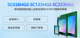
SmartSens SmartGS™-2 Plus series CMOS image sensor products enable intelligent robot vision systems​


With the continuous upgrading of artificial intelligence, machine learning and sensor technology, the robotics industry has entered a stage of rapid development. The application areas and functions of intelligent robots are constantly expanding. More and more intelligent robots of different forms, such as embodied robots, robot dogs, drones, industrial robotic arms, etc., are appearing in people's daily lives. From housework assistance to medical delivery to agricultural automation, intelligent robots have played an important role in various fields such as home, medical care, agriculture, and rescue.

In actual work, intelligent robots need to constantly interact with the real world. Clear, accurate, efficient and stable visual perception capabilities are the key to helping robots complete real-world interactions such as obstacle avoidance and positioning, just like the robot's "electronic eye". SmartSens, a leading CMOS image sensor supplier, has launched a series of products based on the SmartGS™-2 Plus technology platform, including SC038HGS (0.3MP), SC133HGS (1.3MP) and SC233HGS (2.3MP). They have multiple performance advantages such as high sensitivity, high dynamic range and high frame rate. Their excellent imaging effects can fully meet the obstacle avoidance recognition and 3D positioning perception needs of various types of intelligent robots, helping robots achieve accurate real-world interactions.​

1740063998379.png

Please, Log in or Register to view URLs content!
 

tokenanalyst

Brigadier
Registered Member

Chinese scientists achieve major breakthrough in semiconductor quantum dots and CMOS compatible chips!​


The Shanghai Institute of Microsystem and Information Technology of the Chinese Academy of Sciences has made an important breakthrough and successfully realized the heterogeneous integration of III-V semiconductor quantum dot light sources and silicon carbide photonic chips compatible with CMOS processes. This innovative hybrid integration solution precisely stacks GaAs waveguides containing InAs quantum dots onto microring resonators made of 4H-SiC electro-optical materials to form a planar localized light field in the whispering gallery mode.
In further research, after integrating a micro-heater on the chip, the researchers achieved tuning of the spectral range of the quantum dot exciton state up to 4nm. This on-chip thermo-optical tuning capability enables precise matching of the cavity mode with the quantum dot optical signal, achieving microcavity-enhanced deterministic single photon emission. Experiments have shown that this technology has the potential to be expanded on 4H-SiC photonic chips and can overcome the problems caused by the inherent frequency differences between different microcavities.
This new technology combines high purity and CMOS process compatibility, and is expected to promote the development of practical optical quantum networks.

Please, Log in or Register to view URLs content!
 

tokenanalyst

Brigadier
Registered Member

Puzhao Materials completes its B round of financing​


Recently, according to Hunan Puzhao Information Materials Co., Ltd., Puzhao Materials has completed a round B financing of 740 million yuan. This is the second round of financing completed by Puzhao Materials within one year after the 560 million yuan round A financing in early 2024.

Hunan Puzhao Information Materials Co., Ltd. is a professional manufacturer engaged in the research and development, production and sales of high-precision photomask substrate materials in China. The company uses the world's most advanced production and testing equipment and process technology, combined with the company's original technology, to build a sputtering chrome plate production line capable of producing various specifications from 75×75mm to 700×800mm. The products are widely used in the production of photomasks for new flat panel display devices, integrated circuits, fine optics, circuit boards, micro-nano processing, laser anti-counterfeiting and other industries .

In order to break the monopoly of foreign companies, Puzhao Materials has been actively engaged in the research and development, production and technological innovation of mask substrate materials since its inception. Up to now, it has completed the development, certification and mass production and sales of more than 100 product models, and continues to lead in core technologies such as precision grinding, chemical mechanical polishing, SPIN cleaning, magnetron sputtering coating and photoresist spin coating . It has won the National High-tech Industrialization Ten-Year Achievement Award, and its products are exported to overseas countries such as the United States, Germany, South Korea, and Japan.

Puzhao Materials, as a key enterprise of strategic emerging industries under the group, is investing in the construction of a high-precision quartz mask substrate project to improve the domestic industrial chain and accelerate the transformation and upgrading of the mask substrate manufacturing industry. The first phase will invest 800 million yuan (corresponding to the A round of financing) to realize the research and development and industrialization of mask substrates for domestic 8.5-generation flat panel displays. The project has now started construction; the second phase will invest 1 billion yuan (corresponding to the B round of financing) to realize the research and development and industrialization of mask substrates for domestic 28nm semiconductors. After the project is put into production, it will greatly enhance the production capacity and technical level of Puzhao Materials and contribute to the national semiconductor and flat panel display industries.
1740068709891.png

Please, Log in or Register to view URLs content!
 

tokenanalyst

Brigadier
Registered Member

Benefiting from the accelerated domestic substitution of semiconductor equipment parts, Pioneer Precision's net profit in 2024 will increase by 171% year-on-year​


Pioneer Precision achieved a total operating revenue of 1.136 billion yuan in 2024, a year-on-year increase of 103.72%; the net profit attributable to the parent company's owners was 217 million yuan, a year-on-year increase of 170.92%; the non-net profit attributable to the parent company's owners was 217 million yuan, a year-on-year increase of 172.29%.

Regarding the reasons for the performance growth, Pioneer Precision explained that during the reporting period, the company's total operating revenue, operating profit, total profit, net profit attributable to the parent company's owners, net profit attributable to the parent company's owners after deducting non-recurring gains and losses, and basic earnings per share increased by 103.72%, 177.03%, 178.11%, 170.92%, 172.29% and 169.81% respectively over the same period last year. The main reason is that the company's operating income increased, production capacity utilization increased, fixed costs were diluted, and the company's profit growth was driven by the recovery of market demand in the domestic semiconductor industry and the accelerated domestic substitution of key components of semiconductor equipment.

At the end of the reporting period, the company's total assets increased by 85.19% compared with the beginning of the period. The main reason was that the increase in revenue led to an increase in accounts receivable from customers. In order to meet customer delivery requirements, the company appropriately increased inventory. At the same time, in order to meet the needs of capacity growth, the company increased fixed asset investment. The company's equity attributable to the parent company increased by 99.84% year-on-year, mainly due to the company's initial public offering of new shares in December 2024 to raise funds and increase in net profit attributable to the parent company's owners during the reporting period.

According to a reporter from Securities Times, Pioneer Precision Technology was listed on the A-share market on December 12 last year. Founded in March 2008, the company is one of the earliest companies in China to engage in the research and development and production of precision parts for semiconductor equipment such as high-precision cavities for etching equipment. It mainly provides various high-performance customized products such as cavities, liners, heaters, and gas-distributing plates for domestic semiconductor equipment manufacturers and wafer fabs.

Pioneer Precision was one of the few manufacturers in the world that had mass-produced and supplied key components of domestic etching equipment of 7nm and below. It was also one of the earliest companies in China to grow together with major domestic semiconductor equipment manufacturers, and continued to help Chinese semiconductor equipment companies break the international monopoly. It has become a long-term strategic partner of leading domestic semiconductor equipment manufacturers such as China Micro , North Huachuang , Huahai Qingke, Tuojing Technology, and Yitong Holdings.

Please, Log in or Register to view URLs content!
 

tokenanalyst

Brigadier
Registered Member

Casting light into rulers—PLR3000 series fiber laser interferometer new product launch​


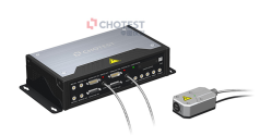
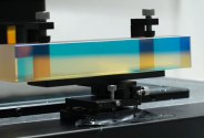
The PLR3000 series fiber laser ruler is based on the principle of laser interferometry. It is an advanced position detection device with high precision, high sensitivity, high efficiency and high speed. It has unparalleled advantages over other measurement methods in the field of non-contact high-precision measurement. Compared with traditional steel tape rulers or glass gratings, it has more accurate grating pitch and higher resolution. At the same time, its heat source isolation design ensures higher stability. It has the characteristics of quick installation and easy alignment. It is specially designed for ultra-high precision position feedback applications and is widely used in modern ultra-precision processing and manufacturing such as microelectronics, micro-mechanics, micro-optics, lithography technology, and high-tech fields such as aerospace.

The PLR3000 fiber laser encoder is equipped with a highly stable He-Ne laser light source with a frequency stabilization accuracy of up to 0.02ppm. The laser is guided by a polarization-maintaining fiber, and the user can easily configure the interferometer to any desired measurement position to minimize Abbe error.
1740086288731.png1740086481818.png


PLR3000 fiber laser encoder can be configured with single-axis, dual-axis and tri-axis output according to user needs, easily realizing multi-axis measurement or multi-degree-of-freedom measurement. At the same time, it provides a variety of interferometric probe configurations. Users can choose corner cube interferometers, plane mirror interferometers, differential interferometers and measurement probes without built-in interferometers according to actual needs to meet users' various complex scene applications.
In addition, we can also customize personalized solutions based on customer application scenarios and help customers solve actual application needs.

2. Features​

● High-resolution digital orthogonal signal output, with a resolution of up to 10nm (externally expandable).
● High measurement accuracy, linear measurement accuracy reaches 0.2~0.5ppm.
● High frequency stabilization accuracy, up to 0.02~0.05ppm.
● Large measuring range, maximum range up to 4m (expandable).
The laser emitting device is separated from the interferometer probe and connected to the cable through a 3m armored optical fiber. The laser ruler host can be kept away from the measured device for easy installation. At the same time, it can also avoid the influence of host heat dissipation on the measurement path.
● Output quadrature digital signal or 1Vpp sine and cosine signal, which can be applied to different controllers.
● Small size, suitable for installation in narrow spaces, can minimize Abbe error.
● It can be used as a laser interferometer for measurement and also for closed-loop position feedback control.
● Multi-channel output can easily realize multi-axis simultaneous measurement and multi-degree-of-freedom measurement.
● Environmental compensation function: the integrated environmental weather station automatically monitors and updates environmental meteorological parameters, and compensates in real time for the effects of temperature, air pressure and humidity on the refractive index of the laser in the air to ensure the accuracy of the measurement.

Please, Log in or Register to view URLs content!
 

tokenanalyst

Brigadier
Registered Member

Pengcheng Semiconductor Glass Substrate TGV Technology Promotes Advanced Packaging​


In the field of advanced packaging, both interposers in 2.5D packaging and 3D packaging use TSV, but recently many people have heard of the term Through Glass Via (TGV). Through Glass Via (TGV) has great potential and may become a common feature of advanced packaging technology in the future. This article will briefly describe the application and development trend of Through Glass Via (TGV) in advanced packaging, as well as a brief introduction to the process.

1740091587557.png

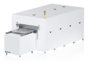
Production TGV/TSV/TMV High Vacuum Magnetron Sputtering Coating Machine​


Glass substrate is the next generation chip substrate, and its core material is made of glass. The key technology of glass substrate packaging is TGV. The glass substrate industry chain includes production, raw materials, equipment, technology, packaging, testing, and application, with the upstream being production, raw materials, and equipment. Due to its unique physical and chemical properties, glass substrates show great potential in the application field of electronic component materials.
The global IC packaging substrate market is developing rapidly, and is expected to reach US$31.54 billion in 2029. Glass substrates are the latest trend, and the penetration rate is expected to reach more than 50% within 5 years. The global glass substrate market has broad space and is expected to grow to US$11.3 billion in 2031. The scale of China's glass substrate market continues to expand, reaching 33.3 billion yuan in 2023. Domestic manufacturers have significant cost advantages, and the localization of glass substrates is accelerating, with huge market space.

Through-Glass Via (TGV) interconnection technology can be traced back to 2008, derived from 2.5D/3D integrated TSV adapter board technology, mainly used to solve the problems of TSV adapter board due to silicon substrate loss, high material cost and complex process. In recent years, the technology has been increasingly improved. Various leading companies have begun to lay out and produce some samples for different fields including: sensors, CPU, GPU, AI, display panels, medical devices, semiconductor advanced packaging, etc.

The advantages of through glass via (TGV) are mainly reflected in:
  1) excellent high-frequency electrical properties.

2) Large-size ultra-thin glass substrates are easy to obtain.

3) Low cost. Benefiting from the easy availability of large-size ultra-thin panel glass and the fact that no insulating layer needs to be deposited, the production cost of a glass adapter plate is only about 1/8 of that of a silicon-based adapter plate.

4) The process is simple. There is no need to deposit an insulating layer on the substrate surface and the inner wall of the TGV, and there is no need to thin the ultra-thin adapter plate;

5) Strong mechanical stability. Even when the thickness of the adapter plate is less than 100µm, the warpage is still small;

6) It has a wide range of applications. It is an emerging vertical interconnection technology used in the field of wafer-level packaging. It provides a new technical approach to achieve the shortest distance and smallest spacing between chips. It has excellent electrical, thermal and mechanical properties. It has unique advantages in RF chips, high-end MEMS sensors, high-density system integration and other fields. It is one of the first choices for the next generation of 5G and 6G high-frequency chip 3D packaging.
Please, Log in or Register to view URLs content!
 

tokenanalyst

Brigadier
Registered Member

HFCVD Hot Wire Chemical Vapor Deposition Equipment.​


We have developed, designed and manufactured hot-filament CVD diamond equipment, which is divided into two categories: experimental equipment and production equipment.
The equipment is mainly used for the development and production of micron-crystalline and nanocrystalline diamond films. It can be used for the development and production of mechanical, thermal, optical and acoustic grade diamond products.
It can manufacture large-sized diamond polycrystalline wafers for heat sinks of high-power devices, high-frequency devices and high-power lasers.
It can be used to produce corrosion-resistant and wear-resistant hard coatings; diamond products for sewage treatment in the environmental protection field.
It can be used for the preparation of diamond films on flat workpieces, and can also be used for the preparation of diamond hard coatings on tool surfaces or other irregular surfaces.
It can be used for the development and production of solar thin-film batteries.

Workpiece size
Circular plane work size: Maximum φ600mm.
Rectangular work size width 1000mm/length can be determined according to the length of the coating chamber (e.g. workpiece length 1500mm).
Equipped with water-cooled sample stage.
Can be coated on one side or both sides.​

1740091796526.png


Please, Log in or Register to view URLs content!
 

OptimusLion

Junior Member
Registered Member
Pinejie Semiconductor received nearly 500 million yuan in financing, and 8-inch silicon carbide will be mass-produced in Q4


Pinejie Semiconductor (Zhejiang) Co., Ltd. officially announced that it had completed the A2 and A3 rounds of financing totaling nearly 500 million yuan. The main investors include Ningbo Tongshang Fund, Ningbo Yongcheng Asset Management, Shanghai Semiconductor Equipment Materials Industry Investment Fund, Nanjing Venture Capital, Shanzheng Innovation, Kuntai Capital, etc. The successful completion of this financing not only demonstrates the capital market's high recognition of Pinejie's technical strength and market prospects, but also indicates that Pinejie has seized a key position in the wave of silicon carbide industry upgrades and is about to open a new chapter of development

Please, Log in or Register to view URLs content!
 
Top