Chinese semiconductor thread II

tokenanalyst

Brigadier
Registered Member
Any update on what happened to smee duv machine for 28nm? Is it still not being released?

I feel all the progress on AI and others mean nothing if China cannot break the lithography chokehold.
You should read the thread before asking questions and ct, there is a neat search button in the top of the page.

For the record, the guy who is talking is from Huazhong University of Science and Technology (HUST) and it seems thay developed an active anti-vibration platform for lithographic machines.

This conference was held in July this year (so already half year ago).

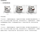
In one of the pictures, they refer to a 28nm litho machine that uses their anti-vibration system: it is visible the brand (a bit blurred), is a SMEE machine!

View attachment 141923

Definitively looks like nothing that they have in their website and looks like they have some innovations because they didn't follow ASML scanners geometry.
View attachment 141929

View attachment 141930

so this is first public image of SSA800i scanner .. wow
 

tokenanalyst

Brigadier
Registered Member

With the increase in sales of CMP products, Huahai Qingke's net profit in 2024 is expected to increase by 34.02% to 49.22% year-on-year.​


Huahai Qingke released its 2024 annual performance forecast, saying that it expects to achieve annual operating income of 335,000 million yuan to 375,000 million yuan in 2024, an increase of 84,200.89 million yuan to 124,200.89 million yuan compared with the same period last year, a year-on-year increase of 33.57% to 49.52%.
It is estimated that the net profit attributable to the owners of the parent company in 2024 will be between RMB 970 million and RMB 1.08 billion, an increase of RMB 246.2534 million to RMB 356.2534 million compared with the same period last year, a year-on-year increase of 34.02% to 49.22%.
It is estimated that the net profit attributable to the owners of the parent company after deducting non-recurring gains and losses in 2024 will be RMB 820 million to RMB 910 million, an increase of RMB 211.8789 million to RMB 301.8789 million compared with the same period last year, a year-on-year increase of 34.84% to 49.64%.
In the same period last year, Huahai Qingke achieved operating income of RMB 250,799.11 million, net profit attributable to the parent company's owners was RMB 72,374.66 million, and net profit attributable to the parent company's owners after deducting non-recurring gains and losses was RMB 60,812.11 million.
Regarding the reasons for the performance changes in 2024, Huahai Qingke explained as follows:
1. The company successfully seized market opportunities by relying on its product technology advantages. The market share and sales scale of CMP products continued to increase, effectively ensuring the steady growth of operating performance;
2. The company continued to increase its R&D investment and production capacity building to enhance its core competitiveness. The R&D and sales of new products progressed smoothly. Thinning equipment, cleaning equipment, wafer regeneration, CDS and SDS began to show initial market results, which increased the company's revenue and profit scale.

Please, Log in or Register to view URLs content!
 

Wahid145

Junior Member
Registered Member
Please, Log in or Register to view URLs content!

so this is summary I guess of the Nikkei article about China's current HBM supply chain. Looks like Tongfu, CXMT and BOE are all working on HBM2. Makes a lot of sense for Tongfu to be working on this. I think I read about it more than a year ago.
I saw the news quite often too about TongFu getting involved with HBM. But what I always wondered is, who is their DRAM chip supplier since AFAIK they just stack the Chips in general (which is one of the core components of HBM).

The other interesting bit is how Display companies are trying to curve out a niche into this HBM bandwagon. Not sure about what Glass substrate this article is talking about is and how it plays a role in HBM. But it would be amazing if a giant like BOE can explore into IC through this HBM venture. Imagine a company like BOE making 14nm Chip (I know this is a far fetched wild dream for now)
 

tokenanalyst

Brigadier
Registered Member
This could be a game changing for homemade lithography

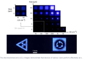
Engineers develop first deep-UV microLED display chips for maskless photolithography​


1737735788594.png

In a breakthrough set to revolutionize the semiconductor industry, the School of Engineering of the Hong Kong University of Science and Technology (HKUST) has developed the world's first-of-its-kind deep-ultraviolet (UVC) microLED display array for lithography machines. This enhanced efficiency UVC microLED has showcased the viability of a lowered cost maskless photolithography through the provision of adequate light output power density, enabling exposure of photoresist films in a shorter time.

Conducted under the supervision of Prof. Kwok Hoi-Sing, Founding Director of the State Key Laboratory of Advanced Displays and Optoelectronics Technologies at HKUST, the study was a collaborative effort with the Southern University of Science and Technology, and the Suzhou Institute of Nanotechnology of the Chinese Academy of Sciences.

A lithography machine is crucial equipment for semiconductor manufacturing, applying short-wavelength ultraviolet light to make integrated circuit chips with various layouts. However, traditional mercury lamps and deep ultraviolet LED light sources have shortcomings such as large device size, low resolution, high energy consumption, low light efficiency, and insufficient optical power density.

To overcome these challenges, the research team built a maskless lithography prototype platform and used it to fabricate the first microLED device by using deep UV microLED with maskless exposure, improving optical extraction efficiency, heat distribution performance, and epitaxial stress relief during the production process.

Please, Log in or Register to view URLs content!
 

tokenanalyst

Brigadier
Registered Member

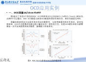
Oriental Jingyuan has proposed the HPO (Holistic Process Optimization) yield maximization technology route and product design concept.​


The collaborative optimization of design and manufacturing processes (DTCO) is the current mainstream solution to the yield problem in the industry. HPO is based on the development of DTCO, and its core is to maximize the yield in the wafer manufacturing process through comprehensive process optimization. Through HPO, Oriental Jingyuan can help users effectively lower the threshold of chip manufacturing, so that they can also manufacture high-end chips through collaborative optimization under the support of a relatively limited supply chain. This is particularly important for China's semiconductor industry in the post-Moore era.

The implementation of the HPO concept is also of great significance to Dongfang Jingyuan itself. After years of development, based on the HPO concept, Dongfang Jingyuan has achieved deep binding with customers. It not only provides point tools according to customers' existing needs, but also strives to string these tools together to provide customers with a new systematic yield management solution. During the interview, Dongfang Jingyuan made an analogy that the HPO integrated yield solution is somewhat similar to the Hong Kong-Zhuhai-Macao Bridge. The company's computational lithography software products, electron beam equipment, yield management software and other point tools are all bridge piers or relay islands. After nearly 10 years of hard work, now all the "bridge piers" have been erected, and they will be effectively connected in the future to build a "cross-sea bridge".

Please, Log in or Register to view URLs content!
 
Top