Chinese semiconductor thread II

tokenanalyst

Brigadier
Registered Member
Interesting.

Generation of continuous extreme ultraviolet laser​


Generating laser with short wavelength is a bottleneck problem in laser technology. The current applicable table-top extreme ultraviolet (EUV) lasers are all generated by multi-photon processes with low efficiency, which cannot produce continuous short wavelength EUV lasers. High density metastable helium atoms are generated by high voltage direct current (HVDC) discharge excitation, and then a continuous extreme ultraviolet laser with a wavelength of 58.4 nm can be produced by combining a continuous near-infrared (NIR) pumped laser to pump the metastable helium atoms to the excited state and then back to the ground state. This process is called single-photon related anti-Stokes Raman scattering (ASRS).
The flux of the EUV laser can approach the current value of synchrotron radiation in this band, which is 2×10¹¹ ph/s. The spot distribution of the generated extreme ultraviolet light is measured, and it is found that some of it has almost the same divergence as the pumped near infrared laser, which is produced by stimulated radiation. The other part is isotropic spontaneous radiation with the same divergence as the extreme ultraviolet light produced by the plasma. Through the change of DC discharge power, it is found that the intensity of the generated extreme ultraviolet laser increases with the increase of discharge power, and the power absorption of the continuous near-infrared pumped laser increases with the increase of discharge power. By changing the wavelength of the NIR laser to observe the above experimental phenomenon, it can be seen that the absorption of the infrared laser power is positively correlated with the generation of the extreme ultraviolet laser intensity, indicating that the enhancement of the extreme ultraviolet light is not caused by the thermal effect of the infrared laser, but the resonance pumping between the metastable and excited states of the continuous NIR laser makes the generation of the extreme ultraviolet laser. Through the change of the injection power of the continuous near-infrared pumping laser, it is observed that with the increase of the injection power of the continuous near-infrared pumping laser, the intensity of the generated extreme ultraviolet laser also increases, but the corresponding production efficiency slowly decreases, which is theorized to be due to the fact that the metastable atomic density increase rate cannot match after the laser pumping. Through the change of helium pressure, it is observed that the extreme ultraviolet laser has the best helium pressure value at a certain discharge power and continuous near-infrared pumped laser injection power.
This is because the increase rate of metastable states density has a certain relationship with the electric power and helium pressure, and the extreme ultraviolet laser intensity is affected by the pump laser, so the optimal helium pressure point exists. Compared with the EUV light generated by traditional high power pulsed seed laser, the CW EUV laser source has the characteristics of high total light intensity and low instantaneous light intensity. This light source is expected to suppress the space charge effect caused by high peak power light sources in photoelectron spectroscopy measurements. Our results provide a possible method for the desktop CW EUV laser by single photon process upconversion

Please, Log in or Register to view URLs content!
 

tonyget

Senior Member
Registered Member
Just saw this news,one of the largest chip manufacture of Russia has been attacked by Ukraine drone,the production is suspended due to this.

I think China should learn some lesson from this. That is,don't build all fabs in coastal cities. It's better to build more fabs in inland areas, they should also build some fabs deep underground just like military factories,to ensure sustained supply of crucial semiconductors during a prolonged war


Please, Log in or Register to view URLs content!

The Silicon El plant stopped working due to the attacks of the Ukrainian Armed Forces: what it means for the Russian Federation

What is known about the strike on the Silicon El plant on Friday, January 24

Baza reports that several drones fell in the area of the microelectronics enterprise JSC "Silicon El" on Krasnoarmeyskaya Street. The plant was suspended after a drone attack, the press service of the enterprise reported.

"On the night of January 23-24, six UAV arrivals were recorded, as a result of which part of the production premises, as well as a finished product warehouse, were damaged. Special energy supply facilities were damaged, and technological production chains were disrupted. The company's activities have been suspended, " the statement reads.

The company "Silicon El Group" is one of the largest manufacturers of chips for the defense industry, produces integrated circuits, discrete semiconductors, silicon structures, power modules, and is engaged in the processing of metals and thermoplastics. More than 1,500 product samples are delivered to 815 enterprises. The staff exceeds 1.7 thousand people.
 

gelgoog

Lieutenant General
Registered Member
Here is the TASS press release.
Please, Log in or Register to view URLs content!

Here is their website.
Please, Log in or Register to view URLs content!

Seems to be mostly power electronics. Some for automotive. Makes sense since Bryansk is where the Bryansk Automobile Plant (BAZ) which makes the trucks for the S-400 SAM is located.

Please, Log in or Register to view URLs content!
JSC Gruppa Kremniy El is the second-largest microelectronics manufacturer in Russia, and, in particular, a manufacturer of microchips. The microchips produced by JSC Gruppa Kremniy El in its plant are used by the Russian military for several purposes, including in the Iskander ballistic missiles. The company is also a part of the Russian federal program “Alternative”, which aims to develop new radars on active phased arrays, intended for air defence and to be installed on aircraft and ships. Therefore, JSC Gruppa Kremniy El is responsible for supporting, materially or financially, actions which undermined or threatened the territorial integrity, sovereignty and independence of Ukraine.

Modern drone attacks make it difficult to defend such industrial sites. There simply aren't enough SAM systems to cover everything nor enough missiles. For example to intercept six drones requires on average twelve missiles (two missiles are fired per target). Russia seems to be working on new and modified air defense systems specific against drones. One example is the quad-packed mini missiles for the Pantsir.
 
Last edited:

huemens

Junior Member
Registered Member
TechInsights’ Comments on CXMT:

- CXMT has skipped the 17nm (D1y) node and directly transitioned to the 16nm (D1z) node.
- It is actively working on next-generation DRAM technology, including HBM, even for sub-15nm nodes without EUV lithography.

Key Takeaways:
- Despite the technological gap, CXMT has achieved a high bit density of 0.239 Gb/mm² at the D1z technology node, competing with major manufacturers.
- CXMT’s success in DDR5, now the mainstream technology in the DRAM market, highlights its potential to expand its market share in the global DRAM industry.
cxmt_ddr5_techinsights.jpeg
Comparison of CXMT DRAM generations
cxmt_g4_techinsights.jpeg
 
Last edited:

huemens

Junior Member
Registered Member

Posting here for the record (Tweets can get deleted).
YMTC V9 NAND Analysis by TechInsights

- This chip has the highest vertical gate density among current commercial products and has successfully implemented a 2yy-layer 3D NAND structure.
- The chip demonstrates YMTC’s technological advancement despite U.S. sanctions.
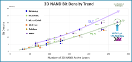
- YMTC maintains its technology of connecting two wafers using a hybrid bonding method and has improved the TLC NAND bit density to over 20 Gb/mm² with this chip.
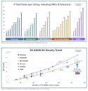
- The graphs show YMTC’s total gate count and 3D NAND bit density compared to competitors (Samsung, SK hynix, Micron, etc.), highlighting significant technological progress.
- YMTC’s 2yy-layer chip includes high-density bits not yet introduced to the market by competitors, indicating a major advancement for China’s semiconductor industry.
ymtc_techinsights.jpeg
 

tonyget

Senior Member
Registered Member
Please, Log in or Register to view URLs content!

TechInsights Finds YMTC 2yy-layered 3D NAND—the Highest TLC Bit Density Ever!

Today, TechInsights found and confirmed China's Yangtze Memory Technology Corporation’s (YMTC) latest and most advanced chip, Xtacking4.x 2yyL 1 Tb 3D TLC NAND. This chip which has the highest number of vertical gates seen in a commercial product to date. YMTC successfully extended the Xtacking 4.0 memory architecture to 2yy-layered 3D NAND devices despite severe U.S. sanctions against the company. It’s the first 2yy-layered 3D NAND device TechInsights has found on the market. We’re in the process of sourcing 2yy-layer (for example 286L) products fabricated from Samsung and Micron. SK hynix’s 321-layer 4D PUC NAND devices are expected to be on the market in H1 2025 as per TechInsights’ 3D NAND Technology Roadmap. Yet, the important takeaway is that China’s YMTC has beat the competition to the market with the TLC bit density found in this device.

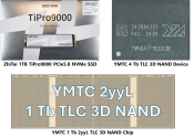
Figure 1. YMTC 2yy-layered 1Tb TLC 3D NAND chip found in the ZhiTai TiPro9000 SSD.png

YMTC’s new Xtacking4.x chip, torn down from the ZhiTai SSD TiPro9000 ZTSS3CB08B34MC, has the YMTC Xtacking4.x structure and design (Figure 1). It consists of 2yy active layers (294L total gates except SGD), 150 gates for the lower deck, and 144 for the upper deck (Figure 2). YMTC maintains its direct bonding (hybrid-bonded) Xtacking structure with two wafers. The previous Xtacking4.0 160L TLC structure consists of 180 total gates including selectors and dummy gates (except SGD). Vertical channel layouts differ slightly from the previous Xtacking4.0 160L; however, the TLC NAND bit density increases to more than 20 Gb/mm2 for the first time in the industry (Figure 3). We estimate the number of active WLs would be around 270.

The YMTC 2yyL 1 Tb 3D NAND die design shows a Center-XDEC design, and the select gate (Poly-Si) on the drain side (SGD) is integrated separately on top of the cell array gates. The backside source connect (BSSC) scheme is still used for the 2yyL structure.

Figure 2. Total number of gates in a 3D vertical NAND string, including YMTC 2yyL.png

Figure 3. 3D NAND bit density trend (TLC and QLC) including YMTC 2yyL 1Tb TLC chip.png

When YMTC released Xtacking4.0 devices (for example, 160L) last year, we expected YMTC would combine Xtacking4.0 technology with higher layers such as 2xxL and 2yyL. . Because of the U.S. ban, YMTC has been unable to extend 3D NAND fabs and import advanced semiconductor equipment and tools. They needed a detour. With the new Xtacking4.0 technology, YMTC appears to have found a way to overcome the current bans with this new chip.

Our technical analysis teams will continue digging into the materials, process integration, and chip design and publishing our findings on the TechInsights Platform as they come available. Please stay tuned.
 

tonyget

Senior Member
Registered Member
Please, Log in or Register to view URLs content!

First China-made DDR5 Memory Released from CXMT China, DDR5-6000 with 16nm DRAM Node!

Amid DDR5 is now highest volume technology, China’s leading DRAM maker, ChangXin Memory Technologies (CXMT) finally revealed 16Gb DDR5 chips to the market. Just this week, TechInsights tore down and analyzed a commercial device which revealed this finding. The Gloway 16GBx2 DDR5-6000 UDIMM (VGM5UC60C36AG-DVDYBN) consists of sixteen16Gb DDR5 devices manufactured from CXMT (Figure 1). The 16Gb DDR5 chip size measures 66.99 mm2 (length 8.19 mm, width 8.18 mm, die sealed) which results in 0.239 Gb/mm2 bit density. The die has CXMT’s new and advanced G4 DRAM generation with 0.0020 µm2 cell size and 16.0 nm feature size (F). CXMT reduced DRAM cell size by 20% from the previous G3 (F=18.0nm) DRAM node (Table 1). Cell pitches measure 29.8 nm, 41.7 nm, and 47.9 nm for active, wordline, and bitline for each, which is corresponding to D1z (F: 15.8 ~ 16.2 nm) generations from Samsung, SK hynix, and Micron. CXMT provides DDR3L (2Gb/4Gb), DDR4 (4Gb/8Gb), LPDDR4X (6Gb/8Gb), and LPDDR5 (12Gb), and has now added DDR5 DRAM devices. The memory maker initially produced G1 DRAM generation with 23.8 nm (D2y) and then G2 with 18.0 nm (D1x).

蜂蜜浏览器_Figure1. CXMT 16Gb DDR5 chip found from Gloway DDR5-6000 UDIMM.jpg

Table 1. Comparison of CXMT DRAM generations, G1 through G4.png

Regarding the DRAM market, DDR5 shipment already crossed over DDR4 in Q2 2024. In 2024, DDR5 shipments reached 87 exabits (vs. DDR4 62 exabits), and expect to be 150 exabits (57%) in 2025 – according to TechInsights’ DRAM Market Report from 4Q2024. DDR5 is now the highest volume technology shipping and will remain so through 2027. Although, the U.S. ban against China restricts use 18nm or smaller DRAM devices and related technology development, CXMT successfully developed and released commercial DDR5 DRAM products with advanced technology node (16.0 nm) for consumption in the domestic Chinese market.

The top three DRAM players (Samsung, SK hynix, and Micron) produce DDR5 devices with more advanced technology nodes such as D1a/D1α and D1b/D1β, having 12 to 14nm feature sizes. Currently, 16Gb chips are the highest volume part. The top three DRAM makers started 16Gb DDR5 mass-production in 2021, which means there is now a three-year technology gapbetween CXMT and these vendors. However, CXMT skipped 17nm (D1y) DRAM node andjumped directly into 16nm (D1z) node. The Chinese chip maker has been aggressively developing the next generation (sub-15 nm without EUV lithography), and HBM technology as well. Our technical analysis teams will continue digging into the materials, process integration, and chip design and publishing our findings on the TechInsights Platform as they come available. Please stay tuned.

Table 2. Comparison of 16Gb DDR5 products from Samsung, SK hynix, Micron, and CXMT.png
 

tokenanalyst

Brigadier
Registered Member

Domestic advanced packaging dark horse joins forces with Huawei!​


Yongsi Electronics confirmed on the investor relations platform on January 22 that the company focuses on the mid-to-high-end advanced packaging field and is committed to implementing a strategy centered on major customers. This move not only demonstrates its positioning in the high-end market, but also arouses widespread attention in the industry about the prospects of its cooperation with Huawei. The latest developments of Yongsi Electronics show that it has become a direct supplier of Huawei HiSilicon chips , especially in mobile phone IC packaging. With the rapid development of 5G technology and the increasing demand for smart devices, the market demand for RF modules has also risen. Yongsi Electronics is actively expanding this field and plans to provide Huawei with corresponding products in the future .

It is expected that in 2023, the company has passed Huawei's supply chain audit and completed proofing, marking an important step in the high-end packaging market. Regarding the capacity issue of the Phase II production line that investors are concerned about, Yongsi Electronics said that the company will continue to work hard to improve its customer service capabilities and core competitiveness. The cooperation with Huawei will prompt Yongsi Electronics to accelerate technological progress and capacity improvement, and promote its further development in the high-end packaging market. In the past few years, Yongsi Electronics has achieved certain results in technology accumulation and market development. Its focus on high-quality and high-performance packaging products not only meets the needs of the domestic market, but also lays the foundation for its entry into the international market. The company's core products cover mobile phone ICs, RF modules and other high-end packaging solutions, which enables it to find room for survival and development in an increasingly complex market environment. Overall, the cooperation between Yongsi Electronics and Huawei is not only an opportunity for the company's development, but also reflects the industry's growing demand for high-end packaging technology. In the future, with the advent of more high-tech products, Yongsi Electronics' performance in the field of mid-to-high-end packaging will be more highly expected.

Please, Log in or Register to view URLs content!
 
Top