You are using an out of date browser. It may not display this or other websites correctly.
You should upgrade or use an alternative browser.
You should upgrade or use an alternative browser.
Chinese semiconductor thread II
- Thread starter vincent
- Start date
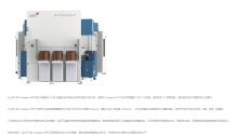
Signed contract for annual production of 100 sets of semiconductor special gas equipment project
A signing ceremony for a project to produce 100 sets of special equipment for semiconductor special gases annually, attracted by the Science and Technology Investment Group, was held.
It is reported that the project investor is headquartered in Shanghai and is a company specializing in the production of ultra-pure clean electrolytic polishing (EP) tubes that meet the international semiconductor SEMI standard. The company team has a full set of technologies from high-performance, high-quality ultra-pure clean stainless steel raw materials to the production and manufacturing of high-quality seamless steel pipes to the final UHP-EP grade electrolytic polishing. The UHP-EP tubes produced are fully in line with the various indicators specified in the international SEMI standards. The project settled in the new district has a fixed investment of 170 million yuan. After full production, it is expected to achieve an annual sales income of more than 100 million yuan and an annual tax payment of more than 5 million yuan.
Hisense releases the world's first 116-inch RGB-MiniLED TV, with color performance surpassing QD-OLED
Beijing time, before the opening of the CES 2025 exhibition, Hisense held a 2025 display technology launch conference, launching the world's first RGB three-dimensional color control LCD display technology. It also exhibited the world's first and largest 116-inch RGB-Mini LED TV using this technology at CES.
Hisense RGB-MiniLED TV is equipped with Hisense's self-developed new generation Xinxin AI picture quality chip, which is also the world's first RGB light and color simultaneous control picture quality chip, breaking through the industry's light and color simultaneous control problem for the first time. Its hardware computing power's CPU single-core performance has increased by 40%, and its scene perception computing ability has increased by 70%. The more powerful AI computing picture quality capability provides the basis for more complex 3*26bits high-precision color control. Hisense's upgraded RGB light and color simultaneous control picture quality chip adopts a dual light control architecture of RGB backlight and LCD panel, redefining the color management system, and realizing precise control of RGB multi-primary color display colors from AI analysis and recognition of display scenes, to AI adaptive light control, and then to high-precision color control.
In order to realize the mass production application of RGB three-dimensional color-controlled liquid crystal display technology, Hisense relies on Qianzhao Optoelectronics to develop the world's leading high-performance RGB-Mini LED backlight chip, and overcomes the key bottlenecks such as efficiency, life, color deviation, and color purity in the application of LED three-color chips, and is the first to achieve the industrialization of three-primary color light source backlight.
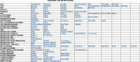
Actually I'm well aware of these companies you mentioned (not all of them tbh) and constantly keeping a track on Google Sheets I made a few years ago. It includes the revenue growth of companies like Huawei, AMAT, Naura, LAM, Piotec, AMEC etc. Just to see the pattern in growth in Domestic vs those 3 American 3 Japanese (TEL, Nikon, Canon) and one Dutch company.There already 3 companies offering high end Ion Implanters with high throughput and variety from High energy to High current. There are only few etching and depositions tools that are not domestically produced even AMEC is getting into and those are for next gen process 3nm like Ruthenium deposition tools.
We have already two threads discussing this one with 3500+ pages and the other with 640+ pages, they have everything, in theory China should be able to make 7nm finfet transistors on their own already.
For Ion Implantation you have: Wanye, CETC and SRI-I
Metrology: SMEE, RainTree,DJEL, angstrom-e, Jingce... cover overlay, CDSEM, ADI, AEI,optical ,XRAY.....
Coating: KingSemi offers immersion lithography coat and developing tools
With the exception of lithography I don't really think not very much difference between tools for a 28nm process and a 7nm process except throughput and you can solve that with more tools. Ion Implanters in China can cover the next gen transistors
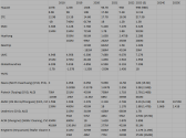

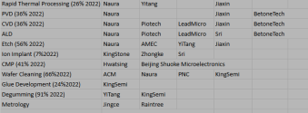
Here's an editable version of the Sheets if anyone wants to see and add some updates just like @tokenanalyst mentioned.
Does not Include the revenue for 2024 yet!
The other thing is, when we want to see a review of the current state of China SME industry, people can't go through 3500+ pages and 640+ pages. They want all the information condensed in literally 2 pages.
Attachments
Last edited:
The other thing is, when we want to see a review of the current state of China SME industry, people can't go through 3500+ pages and 640+ pages. They want all the information condensed in literally 2 pages.
It would be nice if we could have a stickied checklist post or something.
However, I've seen you around for a while, you should have a rough idea of where China's SME stands if you've been paying attention to the thread.
Xiaomi XRING will be MediaTek based SoC with Mali GPU
It seems Xiaomi is finalizing (although no release date at the moment) its first full SoC, the first one was limited to image enanching.
This will be an almost full smartphone processor:

Almost full processor, because the modem will be from Mediatek. The modem is the most technical part of a smartphone chip, only very few players worldwide have developed a modem in-house (2 of them are Chinese): Apple is almost a decade that is trying to achieve this goal but as of today still uses the Qualcomm's.
Bold move by the bold CEO and founder of Xiaomi: that man has no fear to go face-on directly against US / Qualcomm interests. After the successful SU 7 car it seems he want to double down...
SMIC launches new low-temperature CMOS quantum measurement and control chipset
Chengdu Zhongwei Daxin Technology Co., Ltd. (hereinafter referred to as "Zhongwei Daxin") launched a new "Shushan" series of low-temperature CMOS quantum measurement and control chipset for high-fidelity quantum gate control and parallel fast quantum state reading of large-scale quantum bit arrays .
As a domestic start-up with leading technology in the field of quantum measurement and control, Micro-Daxin recently launched a new "Shushan" series of 2 8 nm low-temperature CMOS quantum measurement and control chipsets , including a total of three chips: " Gongga" K onka superconducting qubit control Chips , " Emei" Emei superconducting qubit reading chip and " Xiling " Xiling silicon-based qubit control chip . In response to the current domestic and foreign quantum chip requirements for high fidelity, low noise, high flexibility and low power consumption, this chipset has been adaptively designed to significantly reduce the interconnection complexity, cost and drift of current quantum measurement and control systems. Among them, the "Xiling" Xiling chip was jointly developed with the University of Electronic Science and Technology of China. It has been accepted by the International Solid State Circuit Conference I SSCC 2025 and will have an on-site technology demonstration in San Francisco in February 2025 .
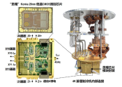
Konka: 28nm Cryo-CMOS superconducting quantum bit manipulation chip SoC
The Konka chip is designed based on the standard 28nm CMOS process, with a chip area of 2mm×3mm, and can work in the 4K temperature range. It contains two quantum control channels on the chip to realize dual quantum gate operation. Each control channel contains a 4~8GHz high-fidelity microwave pulse sequence generation XY channel and a high-precision gate pulse bias Z channel.
Emei: Cryo-CMOS frequency division multiplexing dispersion quantum state reading chip SoC
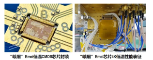
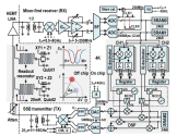
Emei is a 28nm low-temperature CMOS superconducting quantum bit reading chip SoC with a chip area of 2mm×3mm. It can realize parallel frequency division multiplexing FDM quantum state reading of two superconducting quantum bits in the 5.5~8 GHz frequency band. Figure 8 shows the system block diagram of Emei. The chip contains a frequency division multiplexing microwave pulse excitation TX channel, a high linearity low noise mixer pre-RX channel, and matching analog baseband AD/DA and on-chip quantum state demodulation digital signal processing module.
Xiling: Cryo-CMOS high-precision silicon-based quantum bit manipulation chip Soc
Xiling, jointly developed with the University of Electronic Science and Technology of China, is a 65nm low-temperature CMOS high-precision silicon-based quantum bit manipulation chip. It has achieved high-precision manipulation of silicon-based single electron transistor devices at 60mK. The work, titled "Xiling: Cryo-CMOS 18-bit Dual-DAC Manipulator with 4.6μV Precision and 4.1nV/ Hz 0.5 Noise Co-integrated with the Single Electron Transistor at 60mK", was accepted by the International Solid-State Circuits Conference (ISSCC 2025), the top conference in the field of integrated circuit design.
As a domestic start-up with leading technology in the field of quantum measurement and control, Micro-Daxin recently launched a new "Shushan" series of 2 8 nm low-temperature CMOS quantum measurement and control chipsets , including a total of three chips: " Gongga" K onka superconducting qubit control Chips , " Emei" Emei superconducting qubit reading chip and " Xiling " Xiling silicon-based qubit control chip . In response to the current domestic and foreign quantum chip requirements for high fidelity, low noise, high flexibility and low power consumption, this chipset has been adaptively designed to significantly reduce the interconnection complexity, cost and drift of current quantum measurement and control systems. Among them, the "Xiling" Xiling chip was jointly developed with the University of Electronic Science and Technology of China. It has been accepted by the International Solid State Circuit Conference I SSCC 2025 and will have an on-site technology demonstration in San Francisco in February 2025 .
Konka: 28nm Cryo-CMOS superconducting quantum bit manipulation chip SoC
The Konka chip is designed based on the standard 28nm CMOS process, with a chip area of 2mm×3mm, and can work in the 4K temperature range. It contains two quantum control channels on the chip to realize dual quantum gate operation. Each control channel contains a 4~8GHz high-fidelity microwave pulse sequence generation XY channel and a high-precision gate pulse bias Z channel.

Emei: Cryo-CMOS frequency division multiplexing dispersion quantum state reading chip SoC
Emei is a 28nm low-temperature CMOS superconducting quantum bit reading chip SoC with a chip area of 2mm×3mm. It can realize parallel frequency division multiplexing FDM quantum state reading of two superconducting quantum bits in the 5.5~8 GHz frequency band. Figure 8 shows the system block diagram of Emei. The chip contains a frequency division multiplexing microwave pulse excitation TX channel, a high linearity low noise mixer pre-RX channel, and matching analog baseband AD/DA and on-chip quantum state demodulation digital signal processing module.


Xiling: Cryo-CMOS high-precision silicon-based quantum bit manipulation chip Soc
Xiling, jointly developed with the University of Electronic Science and Technology of China, is a 65nm low-temperature CMOS high-precision silicon-based quantum bit manipulation chip. It has achieved high-precision manipulation of silicon-based single electron transistor devices at 60mK. The work, titled "Xiling: Cryo-CMOS 18-bit Dual-DAC Manipulator with 4.6μV Precision and 4.1nV/ Hz 0.5 Noise Co-integrated with the Single Electron Transistor at 60mK", was accepted by the International Solid-State Circuits Conference (ISSCC 2025), the top conference in the field of integrated circuit design.
us govt has ordered the linux foundation to stop working with huawei and tencent:
EUV pellicles developing device.

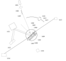
Extreme ultraviolet lithography mask protective film detection device
CN118858161A
CIOMP
Abstract
An EUV photolithography mask protective film detection device comprises: a detection light source module, which is used to generate an EUV light source used for detection, the wavelength of which is in the EUV band, and is equipped with an EUV irradiation time control electronic shutter to control the irradiation time, and a light source transmission system; a sample stage module, which is placed in a vacuum chamber and is used to fix, move and rotate the sample to be tested, so as to realize the switching of different performance detections of the protective film, and to realize the irradiation of the EUV light source at different positions and different incident angles on the protective film; a detection module for the influence of pollutants on the protective film on mask imaging, which is used to study the influence of pollutants of different types and sizes below 50µm, and the distance between the protective film and the mask on the mask imaging, and determine the optimal distance; a protective film transmittance, transmission uniformity and reflectance measurement module, which is used to measure the optical properties of the protective film at different incident angles, and to study the influence of chemical changes of the protective film on its optical properties.
