Chinese semiconductor thread II

tokenanalyst

Brigadier
Registered Member

Shandong releases new materials industry science and technology innovation action plan, with third-generation semiconductor materials and photoresists being the focus.​


The Action Plan proposes to implement a landmark strategic material breakthrough action for the industrial chain. In terms of new generation electronic information materials, research is conducted on the preparation technology and equipment of third generation semiconductor materials such as large-size silicon carbide and gallium nitride, and breakthroughs are made in the core technology of ultra-precision and efficient processing of silicon carbide and gallium nitride substrates. Conquer the ultra-wide bandgap diamond single crystal, aluminum nitride growth and device technology, and break through the large-caliber high-quality silicon single crystal and high-end photoresist preparation technology to meet the independent and controllable technology needs in the integrated circuit and chip industry.

-Artificial crystals. Innovate technologies such as large-size crystal growth, crystal defect suppression, and device design, achieve original theoretical breakthroughs and independent control of technology, and focus on the development of laser and nonlinear optical crystals, piezoelectric/ferroelectric crystals, laser self-frequency doubling crystals, electro-optical crystals, etc., to meet the needs of advanced strategic equipment and major national projects.

-Advanced ceramics. Conquer key core and common technologies in the industry such as ceramic precision forming, additive manufacturing, ultra-precision machining, and device design, focus on developing new structural and functional ceramic materials for extreme scenarios, realize the integrated development of high-end powders, advanced ceramic products, and high-end applications, and create an advanced ceramic innovation and industry highland
.

-New generation of electronic information materials. Research the preparation technology and equipment of third-generation semiconductor materials such as large-size silicon carbide and gallium nitride, and break through the core technology of ultra-precision and efficient processing of silicon carbide and gallium nitride substrates. Conquer the ultra-wide bandgap diamond single crystal, aluminum nitride growth and device technology, break through the large-caliber high-quality silicon single crystal, and high-end photoresist preparation technology to meet the independent and controllable technology needs in the integrated circuit and chip industry.


Please, Log in or Register to view URLs content!
 

tokenanalyst

Brigadier
Registered Member

Precision Electronics (JINGCE): Winning bids for bright field defect detection and other equipment, the turning point of semiconductor measurement business has appeared​


On December 17, the winning results of the 12-inch production line of Nortel Integrated were announced, and Jingce Electronics won the bid for defect inspection machines and stress tester equipment; on December 20, Jingce Electronics announced the signing of a major contract, intending to sell brightfield defect inspection machines and stress testers to customers, with a total order amount of 120 million yuan. Winning the bid

-Brightfield is the category with the highest value and the highest technical threshold for measurement and testing equipment. According to the announcement of Yandong Micro, Nortel Integrated's process node covers 28nm-55nm. This time, the company won the bid for the core brightfield equipment, which strongly proved the company's competitiveness in the field of measurement equipment and broke the market doubts.

-Nortel Integrated is a wholly-owned subsidiary of Beijing Electronics Holdings Co., Ltd. It plans to invest 33 billion yuan to build a 12-inch integrated circuit wafer production line with a planned production capacity of 50,000 pieces/month, and is expected to start production in June 2026. According to the information on China International Bidding Network, the equipment has started bidding. Combined with the planned production time, we believe that 2025 will be the peak period for equipment bidding. Considering that the company's core products have covered processes above 1xnm, film thickness products, OCD equipment and electron beam equipment have obtained repeated orders for advanced processes, and the core bright field equipment has won the bid this time, we are optimistic about the order flexibility brought to the company by the subsequent Nortel integrated bidding.

-The new BIS regulations accelerate the substitution of measurement imports, and the turning point of the company's semiconductor orders has appeared. The implementation of the new BIS regulations, the upgrade of export controls on US semiconductor equipment + the strengthening of restrictions on mainland wafer factories (footnote 5) + avoidance of white gloves (red flag), the above means will undoubtedly accelerate the domestic substitution of equipment. At present, the localization rate of measurement/detection is low, and advanced process bright/dark field and other equipment have not yet achieved a strict breakthrough in mass production. Considering that the US company KLA basically monopolizes the measurement equipment link, it is the most urgent link for domestic substitution.

At present, the core products have covered processes above 1xnm, film thickness products, OCD equipment and electron beam defect review equipment have obtained repeated orders for advanced processes, and semiconductor silicon wafer stress measurement equipment has passed verification and has obtained repeated orders from many domestic head customers. According to the company's third quarter report, bright field defect detection equipment for advanced process nodes has been delivered, and other reserve products such as graphic dark field defect detection equipment are currently in the research and development stage; at the same time, the company has increased its investment in Wuhan Kefu subsidiary and actively deployed advanced packaging. External sanctions have catalyzed the continuous maturity of its own product line, and the company is optimistic about the rapid growth of semiconductor measurement equipment orders in 2025.​
 

tphuang

Lieutenant General
Staff member
Super Moderator
VIP Professional
Registered Member
on Huawei and cameras

H首发国产一英寸主摄,其实也可以算自研CIS,与另一家纯国产CIS厂商合作,有很多自主的核心技术。哦对了,那颗超大底潜望镜也是独家研发

New camera using CIS developed with a fully domestic CIS firm, so smartsens most likely (since Omnivision is not fully domestic).

It's good to see that more Chinese CMOS players getting into things.
 

tokenanalyst

Brigadier
Registered Member

Jingchi Electromechanical's 8-inch silicon carbide resistance crystal growth furnace successfully passed customer verification​


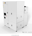
The 8-inch silicon carbide resistive crystal growth furnace launched this time is a new equipment for the preparation of advanced semiconductor materials carefully developed by Jingchi Mechanical and Electrical to meet current market demands.

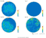
The equipment adopts a unique structural design, combined with the most advanced process control theory and automated control methods, to achieve precise control of process parameters during crystal growth and highly intelligent equipment operation. Through innovative thermal field design, uniform radial temperature and wide range of precisely adjustable axial temperature gradients are achieved. The thermal field has high stability and long service life, which greatly improves the quality and yield of crystals.

1736352060438.png1736352092925.png

Please, Log in or Register to view URLs content!
 

Wahid145

Junior Member
Registered Member
on Huawei and cameras


New camera using CIS developed with a fully domestic CIS firm, so smartsens most likely (since Omnivision is not fully domestic).

It's good to see that more Chinese CMOS players getting into things.
@Awenumick or @curiouscat See if you can access this digitimes link for us. Would be interesting to see how far the the domestic CIS players were able to chip off Sony & Samsung's market share.
Please, Log in or Register to view URLs content!
 

tokenanalyst

Brigadier
Registered Member
A bit of history, China Semiconductor Industry 2006-2015

Mainland China’s IC market is large, with more than 70% relying on imports


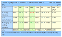
Wang Longxing pointed out that after years of development, mainland China's IC industry has developed vigorously in recent years. From 2006 to 2012, the average annual compound growth rate (CAGR) reached 18.8%, of which the IC design industry reached 25.7%. level; see Table 1 for details.
1736382258149.png

From the data in Table 1, it can be seen that the mainland's semiconductor industry chain has developed quite completely. In addition to establishing an industrial system for the interlocking common development of IC design industry, chip manufacturing industry, packaging and testing industry, and equipment and materials, the industry Each block in the chain has considerable output value and growth rate. It is worth noting that due to the impact of the 2008 financial crisis, the output value of many fields declined in 2009, but the IC design industry did not fall but rose. This shows how strong the growth of the mainland IC design industry is.

In addition to the formation and increasingly complete industrial chain, industrial clusters are also quietly taking shape. Wang Longxing pointed out that in the past few years, mainland China has formed three major industry-intensive areas: the Yangtze River Delta, the Beijing-Tianjin Rim Bohai Bay, and the Pearl River Delta, as well as emerging industrial areas in the central and western regions with Xi'an, Chengdu, Chongqing, and Wuhan as central cities. In summary, there are two major niches for the development of the IC industry in mainland China. The first major niche is the government's strong support for the development of the IC industry, which induces joint efforts by the industry. This also promotes the rapid rise of IC technology levels and actively strives to shorten the gap with the world's advanced technology levels. gap. In terms of technology, according to the 2013 Shanghai Integrated Circuit Industry Development Research Report, China's IC design technology is expected to reach the 22nm/20nm level in 2015, while chip manufacturing can enter the 300mm wafer 32nm complete process; in addition, 28nm has already Enter mass production and break through 22m/20nm key technologies. As for the main IC packaging forms, mainland China will also enter the international mainstream field in 2015 and further improve advanced packaging technologies such as Flipchip, BGA, CSP, WLP and MCP. In addition to expanding the production capacity of advanced packaging forms, it will also accelerate the system Development of high-end packaging and testing technologies such as SiP and 2.5D/3D IC.


The second major niche for the development of the IC industry in the mainland is the huge IC market demand in the mainland, which provides strong support for the development of the IC industry in the mainland. The self-sufficiency ratio of mainland China's IC industry is not high. Table 2 below shows the size of the mainland IC market from 2006 to 2015. From 2007 to 2015, it had a compound annual growth rate of 12.5%. In fact, since 2005, mainland China has become the world's largest single IC market. However, mainland China's local IC production volume is far from keeping up with market demand. Wang Longxing pointed out that last year (2012), the mainland's local system units purchased IC-related products worth US$130 billion, but the mainland's local IC output value was only US$33 billion. Most of the locally produced products are for self-use, and a small part is exported. The self-sufficiency ratio is only about 25%. More than 70% of ICs must be imported. Wang Longxing said: "The mainland market is huge. If it develops, the market will be even bigger. Therefore, we cannot rely entirely on imports. We must cultivate our own R&D and production capabilities. However, we still have to import the latest equipment from abroad. If we develop the latest equipment at a faster speed, we must cultivate our own R&D and production capabilities." If we cannot keep up with technological development, we will still have to rely on imports.”​

Mainland semiconductor equipment manufacturing has achieved breakthrough development

Wang Longxing pointed out that many local semiconductor companies in mainland China are still developing. Whether it is IC design, chip production and manufacturing, or even equipment manufacturing, their scale is not as large as that of large foreign companies. The gap is quite large. "Currently, Taiwan is the mainland's largest partner in the semiconductor field. Many Taiwanese companies, such as packaging and testing, IC design, and wafer packaging manufacturers, are heavily involved in the mainland market, and Taiwan is also the largest importer of mainland ICs." Overall, Wang Longxing believes that China is currently only better than Taiwan in semiconductor equipment and materials, while Taiwan is relatively lacking in this area.

Semiconductor equipment manufacturers in mainland China are divided into two categories. One category is the mainland branches of relatively large internationally renowned manufacturers, such as the American company Applied Material and the Japanese company TEL. Because China is a large equipment market, international Manufacturers do not want to be absent; on the other hand, Wang Longxing pointed out that local equipment manufacturers in mainland China have also grown rapidly in recent years; so far, there are about 50 or 60 large-scale local equipment manufacturers. Most of these large equipment manufacturers are concentrated in Beijing and are state-owned enterprises. Such as Northern Microelectronics, Seven Star Huachuang, Electronic Technology Group 45th Research Institute, etc.; while wafer manufacturing and IC design are concentrated in Shanghai. Wang Longxing said: "Shanghai's equipment factories are all small and medium-sized enterprises. They are not comprehensive, but they are quite professional in a specific field. For example, China Micro Semiconductor's plasma etching machine has reached the 20nm level; in addition, like Shanghai Microelectronics Equipment Company is the only company in the country that manufactures complete lithography machines. The technology sources of these manufacturers include imported from abroad and self-developed. For example, local lithography machines are highly integrated and are supported by many optical research institutes in China. . Many high-precision instruments, such as exposure systems, light source systems, optical radio stations, etc., are supplied by other manufacturers and then integrated by Shanghai Microelectronics.”

Shanghai Microelectronics Equipment Company is the only company in China that can produce complete photolithography machines.

Currently, mainland China does not stipulate the comparison of manufacturers purchasing local equipment, but there is a policy that if the equipment has been successfully developed and passed verification, manufacturers will be recommended and encouraged to purchase it. (Sadly never enforced)

Overall, mainland China has made great progress in the research and development and production of wafer manufacturing equipment, packaging and testing equipment, and semiconductor material processing equipment in recent years, such as 300mm plasma etching machines and 300mm single wafer cleaning machines. Not only has it been selected by local IC production lines, it has also entered the international market; however, the 450mm part has not yet officially started (I here from the future, 450mm never happened). Wang Longxing said: "At present, most of the production lines of local equipment factories are still 200mm, and this quantity is the largest. Some domestic equipment factories cannot even make 200mm equipment. Although 300mm is also developing rapidly, the quantity has not exceeded 200mm. As for the manufacturing process Some 90nm products are quite large, but the quantity of 65nm products is also quite large. In addition, mainland China has also begun to engage in 3D IC, such as Jiangyin Changdian and Nantong Fujitsu, etc., which have begun small-scale production.”

4 years of Think Tank stooge sponsored export controls.

1736382503466.png


JPaladin32

New Member
Registered Member
Got my Mate 70 Pro. The supply situation is actually less bad than I previously thought.

For anyone who's still interested, I launched the debug bridge and probed cpuinfo. In the list of CPU features advertised by the kernel, I found features as high as Armv8.7. The interesting thing is that because many features like SVE2 and SME are optional in Armv9, there's no way to tell if a CPU is v9 but chooses not to implement them, or it's just v8.

Worse, because Kirin 9020 is a mobile SoC and is still 7nm, I doubt Huawei would implement them until there's enough transistor budget, which I would guess will be after EUV.
 
Top