Chinese semiconductor thread II

tokenanalyst

Brigadier
Registered Member

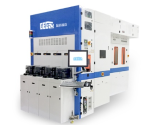
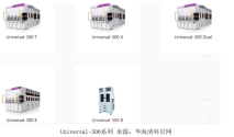
Huahai Qingke's chemical mechanical polishing equipment achieves full coverage of the dielectric layer!​


Huahai Qingke developed China first 12-inch "dry-in and dry-out" CMP equipment and series of products. The overall technology reached the international advanced level, achieved mass production of 28nm process, and had the ability to expand 14-7nm process, creating many domestic equipment records. A total of more than 110 units have been applied to large production lines for advanced integrated circuit manufacturing, and the market share and import substitution rate are both among the top domestic IC equipment. The series of achievements filled the domestic gap, broke the monopoly of international giants, and realized the mass industrialization application of domestic polishing equipment for the first time. At present, the company's chemical mechanical polishing (CMP) equipment has achieved comprehensive coverage of dielectric layers such as polysilicon, silicon dioxide, silicon nitride, and aluminum oxide.
1736294905558.png
 

tokenanalyst

Brigadier
Registered Member

CMP equipment is exported to regions outside of mainland China!​


Beijing Jingyi Precision Technology Co., Ltd. is a joint-stock company established by the overall change of Beijing Shuoke Precision Electronic Equipment Co., Ltd. (Shuoke Precision). It was registered and established in Beijing Economic and Technological Development Zone on September 23, 2019, and is a national high-tech enterprise. The company focuses on the core business of CMP, the core equipment of integrated circuits, and focuses on the technical and operational shortcomings that need to be broken through in the process of industrialization and marketization. It continuously promotes the research and development and industrialization of CMP equipment, continuously strengthens capacity building, builds a business development system, and continuously consolidates core competitiveness.

1736295062177.png

Jingyi Jingwei's CMP equipment achieved the sales of the first exported CMP equipment, which marked an important step for Jingyi Jingwei in the field of high-end semiconductor equipment manufacturing and reflected the increasing influence and competitiveness of domestic key equipment in the global semiconductor industry chain. At the same time, the company revealed that this achievement was achieved thanks to two aspects. First, Jingyi Jingwei has been working in the field of traditional silicon-based ultra-large-scale integrated circuit manufacturing for many years, and has achieved large-scale sales and a large number of product verifications for customers such as SMIC and Unigroup, with a silicon-based tape-out volume of over one million pieces. Second, Jingyi Jingwei's CMP equipment has previously obtained certification and orders from the first 6/8-inch SiC device manufacturer in mainland China, and the tape-out volume is conservatively estimated to exceed 10,000 pieces.​
 

gelgoog

Lieutenant General
Registered Member
FT's 2032 forecasts are likely based on publicly announced future planned capacity increases. I suspect many Chinese fabs have stopped publicly announcing all of their long term expansion plans so as to avoid giving out information that can be used by the US for sanction targeting and enforcement.
FT's forecasts are still retarded. Like you said, a lot of companies stopped announcing their planned expansions. Besides, I published the architect concept designs here, for example Hua Hong Wuxi is starting up Fab 2 (~100k wpm), when the site has space for Fab 3 (~100k wpm) as well. Those 100k wpm SMIC fabs (Beijing, Tianjin, Shanghai) are also on sites which allow building a second 100k wpm fab. In some cases, like the Beijing or Shanghai fab, even more than just a second fab.

YMTC Wuhan and CXMT Hefei also have enough space for a further 100k wpm expansion each, Fab 3, which was also planned to happen in the future.

The way FT lies in plain sight is by using the derivative. Notice it is a % change in capacity in wspm from one time period to the next. So even if their dataset was true (which it likely is not) their chart just states that China will be slowing down its fab construction versus the current construction rate. Not that China will be building less capacity than the others.
 
Last edited:

huemens

Junior Member
Registered Member

interesting rankings here. So YMTC has the most dense 6th and 7th gen NAND

What they have listed for 8th gen is YMTC's old Xtacking 3.0 process. Note their latest process listed in 7th gen is Xtacking 4.0 and it gets top spot with fewer layers than everyone else. So now it's only a matter of them scaling Xtacking 4 to 200+ layers.
 

tphuang

Lieutenant General
Staff member
Super Moderator
VIP Professional
Registered Member
What they have listed for 8th gen is YMTC's old Xtacking 3.0 process. Note their latest process listed in 7th gen is Xtacking 4.0 and it gets top spot with fewer layers than everyone else. So now it's only a matter of them scaling Xtacking 4 to 200+ layers.
well, until they get the domestic tools to work with 232 layers, that's going to continue be an issue.
 

siegecrossbow

General
Staff member
Super Moderator

Xiaomi XRING will be MediaTek based SoC with Mali GPU​


Please, Log in or Register to view URLs content!

It seems Xiaomi is finalizing (although no release date at the moment) its first full SoC, the first one was limited to image enanching.

This will be an almost full smartphone processor:

View attachment 142847

Almost full processor, because the modem will be from Mediatek. The modem is the most technical part of a smartphone chip, only very few players worldwide have developed a modem in-house (2 of them are Chinese): Apple is almost a decade that is trying to achieve this goal but as of today still uses the Qualcomm's.

Bold move by the bold CEO and founder of Xiaomi: that man has no fear to go face-on directly against US / Qualcomm interests. After the successful SU 7 car it seems he want to double down...
Entity list time for Xiaomi.

View attachment 139346
 

tokenanalyst

Brigadier
Registered Member

VeriSilicon Display Processor IP DC8200-FS Obtains ISO 26262 ASIL B Certification​

VeriSilicon (Visilicon, stock code: 688521.SH) today announced that its high-performance, low-power display processor IP DC8200-FS has successfully passed ISO 26262 ASIL B automotive functional safety certification. The certification certificate was issued by TÜV NORD, an international inspection and certification body.
The DC8200-FS IP, which complies with the ISO 26262 ASIL B standard, has a series of advanced safety mechanisms, including memory protection and register configuration path protection. The IP is available in two configuration versions, DC8200-FS 2K and DC8200-FS 4K, which can achieve real-time image processing in pre-processing and post-processing processes, and support dual-output display panels with a resolution of up to 4Kx2K. These outputs are compatible with the MIPI Display Serial Interface (MIPI DSI) interface and DisplayPort (DP) interface, and support RGB and YUV formats. The DC8200-FS IP is also equipped with two AXI buses for efficient access to external frame buffers, and two AHB buses for register programming to ensure seamless system integration. In addition, the software of DC8200-FS supports the mainstream Linux DRM framework, customized drivers and customized API interfaces, which facilitates flexible and customized development of automotive systems.

Please, Log in or Register to view URLs content!
 

tokenanalyst

Brigadier
Registered Member
Nanometer level alignment in nanoimprint lithography

Nanometer stamping wafer high-precision alignment method based on multi-scale image recognition​

Tenren Micro-Nano​

CN118799367A​

Abstract​

The invention discloses a high-precision alignment method of a nanoimprint wafer based on multi-scale image recognition, which belongs to the technical field of image processing, and after the image is grayed, three-scale images are constructed, contours are extracted from the three-scale images respectively, the contours are thinned, so that contour lines are clear, and finding out the coordinates of the mark points according to the bending characteristic values of the contour lines in the images with three scales, combining the images with three scales, improving the precision of finding the coordinates of the mark points, mapping the coordinates of the mark points into the space coordinates, obtaining deviation positions according to the space coordinates, and aligning the wafer based on the deviation positions. According to the method, the outline center point is extracted from the three-scale images, the three-scale refined images are constructed, so that the outline structure is clearer, the accuracy of determining the mark points is improved, the coordinates of the mark points are found by combining the bending characteristic values of the outline under the three scales, and the accuracy of determining the mark points is further improved, so that the alignment accuracy is improved.​
 
Top