You are using an out of date browser. It may not display this or other websites correctly.
You should upgrade or use an alternative browser.
You should upgrade or use an alternative browser.
Chinese semiconductor thread II
- Thread starter vincent
- Start date

I'm not really sure why he didn't just post the entire thing. The 13.5nm EUV light source is clearly provided by HIT to EUV machine. The fact that it won't an order tells me they verified it to a degree on the prototype. So now, it's just about time to get it the machine commercialized. And this is a year end reporting, so it would have likely happened months ago to win the award.
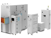
Xinfeng Precision's first 8-inch fully automatic high-precision SiC wafer thinning machine was successfully delivered
Xinfeng Precision Technology Co., Ltd. announced that its first 8-inch fully automatic high-precision silicon carbide (SiC) wafer thinning machine independently developed by it has been successfully delivered to customers. This milestone achievement marks that Xinfeng Precision has made a major breakthrough in the field of ultra-precision grinding technology for hard and brittle materials, breaking the foreign monopoly and filling the gap in this field in China.

The 8-inch fully automatic high-precision silicon carbide wafer thinning machine is a major achievement of the Xinfeng Precision team after intensive research and development and overcoming many technical difficulties. According to the Xinfeng Precision R&D team, the thinning machine uses a number of innovative technologies, including high-precision grinding system, real-time monitoring feedback control, self-developed motion control system and endpoint compensation algorithm, etc., to ensure ultra-high precision and ultra-high stability in the SiC wafer thinning process. Especially in the design of the grinding system, Xinfeng Precision independently developed a special sharp and stable grinding wheel to cope with the high hardness and high brittleness of SiC wafers.
In addition, the thinning machine is also fully automated, with no need for manual intervention from wafer loading, positioning, grinding to unloading, which greatly improves production efficiency and product consistency. At the same time, through real-time monitoring and feedback control, the thinning machine can adjust the angle matching algorithm in real time according to the difference in incoming materials to obtain the best surface accuracy. The successful delivery of the 8-inch fully automatic high-precision silicon carbide wafer thinning machine not only marks a major breakthrough in the field of SiC wafer thinning technology by Xinfeng Precision, but also highlights its leading position in the field of global semiconductor manufacturing equipment.
This is a first,
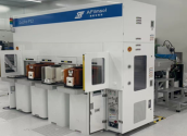
First Semiconductor's first 12-inch PECVD Amorphous Carbon equipment Dubhe delivered to industry-leading customers
Plasma chemical vapor deposition (PECVD) is a core link in semiconductor manufacturing. It is crucial to ensure the process performance of the entire chip and directly determines the reliability and quality of semiconductor devices. Among them, amorphous carbon hard mask (PECVD Carbon) is an important process in realizing the advanced semiconductor process patterning process. This film has a high selective etching ratio for dielectric layer films such as polysilicon, silicon oxide, and silicon nitride, and can support customers to achieve high aspect ratio feature patterning. At the same time, the Carbon film can be easily removed in subsequent processes to improve the yield and reduce the cost of process development. Under the current situation of limited domestic Fab factory lithography machines, this film layer will be widely used in the field of advanced processes in the future. At the same time, this film layer is also suitable for special process requirements in the pan-semiconductor field.
amorphous carbon hard mask (PECVD Carbon) is an important process in realizing the advanced semiconductor process patterning process. This film has a high selective etching ratio for dielectric layer films such as polysilicon, silicon oxide, and silicon nitride, and can support customers to achieve high aspect ratio feature patterning. At the same time, the Carbon film can be easily removed in subsequent processes to improve the yield and reduce the cost of process development. Under the current situation of limited domestic Fab factory lithography machines, this film layer will be widely used in the field of advanced processes in the future. At the same time, this film layer is also suitable for special process requirements in the pan-semiconductor field.

Shouxin Semiconductor's first 12-inch Dubhe series plasma enhanced equipment can correspond to customers' amorphous carbon thin film processes of 90/55/28nm and below, matching the process specifications of similar equipment of mainstream foreign manufacturers, and has the advantages of higher production efficiency and wider process adjustment window. The equipment is equipped with a self-developed RF control system, atmospheric and vacuum transmission platform, and a self-developed software control system. It can match the customer's EAP and MES system integration to assist customers in automated and efficient production. It can be widely used in chip manufacturing fields such as logic chips, memory chips, MEMS, power devices, silicon-based microdisplays, silicon photonics and advanced packaging. At the same time, Shouxin Semiconductor can develop and optimize processes according to customer needs and provide customers with long-term technical support.
Amorphous Carbon is used as a hard mask for FinFETs and Memory. A hard mask is a removable material used to protect the pattern in the etching process SiO2 in the old times.
Huawei continues to make efforts and achieves new breakthrough in diamond heat dissipation!
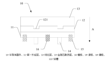
Diamond heat dissipation Semiconductor devices Artificial diamond Power electronics Huawei [Introduction] Huawei: Patent for "a semiconductor device and its manufacturing method, integrated circuit, and electronic device". According to information from the State Intellectual Property Office, Huawei Technologies Co., Ltd. has announced an invention patent titled " A semiconductor device and its manufacturing method, integrated circuit, and electronic device ". The application publication number is CN119069436A, and the application date is May 2023. This patent provides a semiconductor device and its manufacturing method, integrated circuit, and electronic device, which increases the contact area between the diamond heat dissipation layer and the passivation layer, improves the bonding force between the diamond heat dissipation layer and the passivation layer , and improves the heat dissipation efficiency of the semiconductor device by reducing the heat diffusion distance between the diamond heat dissipation layer and the gate.

The semiconductor device may include a first epitaxial layer, a passivation layer and a diamond heat dissipation layer. The passivation layer is located between the first epitaxial layer and the diamond heat dissipation layer. A gate is arranged on the side of the first epitaxial layer facing away from the passivation layer. A groove is arranged on the surface of the side of the passivation layer facing the diamond heat dissipation layer. Along the thickness direction of the semiconductor device, the projection of the groove on the first epitaxial layer covers at least part of the gate. The diamond heat dissipation layer may cover the passivation layer and fill the groove.
View attachment 142274
I'm not really sure why he didn't just post the entire thing. The 13.5nm EUV light source is clearly provided by HIT to EUV machine. The fact that it won't an order tells me they verified it to a degree on the prototype. So now, it's just about time to get it the machine commercialized. And this is a year end reporting, so it would have likely happened months ago to win the award.
LLNL betting on thulium 2 micron laser for next gen LPPEUV. I believe SIOM is also working on thisThe LLNL-led project will investigate the primary hypothesis that energy efficiency of existing EUV lithography sources for semiconductor production can be improved with technology developed for the novel petawatt-class BAT laser, which uses thulium-doped yttrium lithium fluoride as the gain medium through which the power and intensity of laser beams are increased.
The unique central wavelength of thulium-doped yttrium lithium fluoride, lasing at about 2 microns, differs from all other intense lasers that operate at about or less than 1 micron or at 10 microns. The project will be the first exploration of joule-class laser-target coupling at 2 microns.
This is not bad. Looking forward to tech insight teardown to get the dimension numbers.Dismantling of China's first batch of domestic DDR5 memory: Changxin particle single die is 68.06 square millimeters, 40% larger than Samsung

