Chinese semiconductor thread II

MortyandRick

Senior Member
Registered Member
Please, Log in or Register to view URLs content!

Chinese manufacturers are frantically stockpiling semiconductor materials

Chinese companies are scrambling to secure advanced chips and electronic materials from U.S. suppliers before the New Year amid concerns that Washington will impose more export restrictions on the industry, people familiar with the matter told Nikkei Asia.

Suppliers such as DuPont, Entegris and Chemours have seen a surge in orders since November, including a variety of important consumable materials such as chemical mechanical polishing pads, filters, special containers, advanced lubricants and high-end light bulbs for inspection and testing, the sources said.

The Chinese tech industry is also concerned that the U.S. may impose additional restrictions on the use of advanced chipmaking materials and designs, in addition to the restrictions already announced, they added.

"China has been stepping up efforts to find local solutions over the past few years, but the quality of chipmaking materials and consumables from some U.S. suppliers is still much better and more stable than local products," said a chip distributor familiar with the stockpiling campaign.

DuPont provides high-quality polishing pads commonly used in the chemical mechanical polishing process, a key step in chipmaking. Entegris is a global leader in filters and FOUPs (specialized plastic carriers used to hold wafers), while Chemours provides key lubricants used in a variety of machines in a wide range of industries including aerospace.

In addition to snapping up raw materials from U.S. suppliers, Chinese chipmakers and equipment suppliers are scrambling to find alternative sources for high-end consumables, which are mainly controlled by U.S., European and Japanese suppliers, according to Nikkei Asia. These efforts include trying to replace as many foreign suppliers of chemicals and materials as possible with domestic suppliers.

"Customers told me that they are concerned that the supply of some key consumables may be at risk of interruption and asked us to start looking for and verifying a second source as soon as possible," said an executive at a chip production equipment supplier.

The move is in line with China's efforts to reduce its reliance on U.S. suppliers as the technology race between Washington and Beijing intensifies. Huawei, which has been under pressure from the United States for five years, has been a driving force for China to increase its technological self-reliance.

U.S. President Joe Biden's administration announced sweeping new export restrictions this month and added 140 Chinese entities to a trade blacklist, including the country's largest chip equipment manufacturer. Suppliers must complete business arrangements with blacklisted customers by January 2 or January 31, depending on the specific restrictions, after which they will be required to obtain a license to continue doing business with them.

The United States also released an assessment of China's mature chip production supply chain this month, saying that only 17% of American companies can confirm that their products do not contain Chinese chips. The US government said it would ban government agencies from purchasing products or services containing Chinese chips from December 2027.

The Biden administration also launched a Section 301 investigation into China's mature or less advanced semiconductor trade practices this week. However, Biden will not reach a conclusion before leaving office next month, and it is unclear whether the incoming Donald Trump administration will continue the investigation.

Entegris and Chemours declined to comment. DuPont did not respond to Nikkei Asia's request for comment.
Good. Forces Chinese companies to find and advance local solutions.

While US blocking Chinese chips will just increase inflation
 

tokenanalyst

Brigadier
Registered Member

Shenghe Jingwei completed US$700 million in additional private financing to strengthen its 3D multi-chip integration technology layout


On December 31, 2024, Shenghe Jingwei Semiconductor Co., Ltd. (hereinafter referred to as "Shenghe Jingwei") announced that the $700 million private placement financing for patient capital has been efficiently delivered. The new investors include Wuxi Industrial Development Science and Technology Innovation Fund, Jiangyin Binjiang Chengyuan Investment Group, Shanghai Guotou Futeng Capital, Shanghai International Group, Shanghai Lingang New Area Management Committee Xinxin Fund and Lingang Group Digital Science Fund, as well as Social Security Fund Zhongguancun Independent Innovation Fund, China Life Equity Investment, Golden Link, etc.
Since 2014, Shenghe Jingwei has been committed to the manufacturing of 12-inch mid-end silicon wafers, and further provides full-process advanced packaging and testing services such as wafer-level advanced packaging and multi-chip integration processing. Its terminal products are widely used in high-performance computing, artificial intelligence, data centers, automotive electronics, smart phones, 5G communications and other fields.
With the explosion of artificial intelligence and the continuous promotion of the construction of the digital economy, Shenghe Jingwei has unswervingly continued to increase its R&D investment and is committed to promoting the iterative development of three-dimensional multi-chip integrated advanced packaging technology. The company promotes innovation with innovation and improves quality with innovation, constantly breaking through technical bottlenecks, and has now formed a complete technical system and mass production capacity for full-process chip integrated packaging.
On May 19, 2024, Shenghe Jingwei held a groundbreaking ceremony for ultra-high-density interconnected multi-chip integrated packaging and J2C plant in Jiangyin High-tech Zone, Wuxi City. In the same month, in May 2024, the company launched the 3x mask size TSV silicon through-via substrate technology, marking that its chip interconnection advanced packaging technology has entered the sub-micron era, and has the ability to further improve the chip interconnection density, thereby continuing to seize the technological commanding heights and maintain development opportunities. On November 29, 2024, the J2C plant of Shenghe Jingwei's three-dimensional multi-chip integrated packaging project was successfully capped. After the completion of this project, it will rapidly expand the production capacity of projects under construction and enhance Shenghe Jingwei's core competitiveness in cloud computing, data centers, high-end network servers, and high-performance computing HPC.
Shenghe Jingwei said that since it set sail in Jiangyin in the fall of 2014, it has been committed to developing advanced three-dimensional chip integration processing (3DIC) technology, and continuously developing advanced packaging technologies such as smaller pitch, finer line width, multi-layer interconnection, three-dimensional stacking, and multi-chip integration in a larger size range. By systematically improving the chip interconnection density, together with upstream and downstream partners in the advanced integrated circuit manufacturing industry chain, it helps customers continuously improve the integration level of chip products and meet the increasing demand for chip computing power in the era of artificial intelligence.

Please, Log in or Register to view URLs content!
 

tokenanalyst

Brigadier
Registered Member

Tiancheng's advanced 12-inch wafer-level TSV three-dimensional integration production line officially put into production​


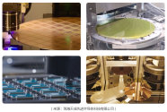
On December 30, 2024, Tiancheng Advanced's 12-inch wafer-level TSV three-dimensional integration production line was officially put into production. This production focuses on three types, a total of six products, based on Tiancheng Advanced's "Nine-fold" wafer-level three-dimensional integration technology system, focusing on the three major technical directions of "vertical and horizontal (2.5D)", "Dongtian (3D)", and "square and round (MicroAssembly)", covering users in multiple fields such as intelligent driving, sensor imaging, and data communication.

1735649894399.png
Tiancheng Advanced is committed to the research and development and innovation of semiconductor wafer three-dimensional integration technology. It has established the industry's first wafer-level three-dimensional integration technology system named in Chinese - "Jiu Chong", focusing on the three major technology series of "Vertical and Horizontal (2.5D)", "Dongtian (3D)", and "Fangyuan (Micro Assembly)". Tiancheng Advanced uses "high aspect ratio TSV silicon through-via technology", "dual damascene RDL rewiring technology", "multi-core integrated large wafer reconstruction technology" and "multi-dimensional interconnection high-density assembly technology" as core technologies to establish a complete mid-process technology architecture and focus on providing users with complete 12-inch system integration and wafer-level advanced packaging solutions .

Please, Log in or Register to view URLs content!
 

tokenanalyst

Brigadier
Registered Member

Shuoke Crystal: The world's first 12-inch (300mm) high-purity semi-insulating silicon carbide substrate​


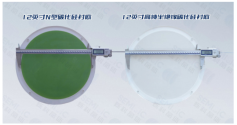
On December 26, 2024, Shanxi Shuoke Crystal Co., Ltd., a subsidiary of China Electronics Technology Group Corporation Semiconductor Materials Co., Ltd., successfully developed a 12-inch (300mm) high-purity semi-insulating silicon carbide single crystal substrate, and at the same time successfully developed a 12-inch (300mm) N-type silicon carbide single crystal substrate.
1735650089345.png
Shuoke Crystal has always focused on the research and development and production of silicon carbide materials, and explored broader application scenarios for silicon carbide materials. It has successively mastered the large-size diameter expansion process, the key process of high-purity semi-insulating silicon carbide substrates, and the growth process of low-defect N-type substrates. The successful development of the world's first 12-inch high-purity semi-insulating silicon carbide substrate will accelerate the further expansion of silicon carbide materials in new application scenarios such as VR glasses and heat sinks.

In the future, Shuoke Crystal will continue to focus on the industrialization technology of large-size silicon carbide single crystal substrates, continue to increase R&D investment, give full play to the leading role of technological innovation, build core competitive advantages, thereby driving the innovation and reconstruction of the innovation chain, industrial chain, and ecological chain, and leading the industry to develop in a more high-end direction.

Please, Log in or Register to view URLs content!
 
Top