You are using an out of date browser. It may not display this or other websites correctly.
You should upgrade or use an alternative browser.
You should upgrade or use an alternative browser.
Chinese semiconductor thread II
- Thread starter vincent
- Start date
VPTEK defect detection tools solutions for TGV and IC
Logic Chip
As the integration of electronic components increases, the demand for testing becomes more stringent. As the core of integrated circuits, the quality of logic chips directly affects the performance of electronic products. Vip's Tornado series products use optical systems and image processing algorithms to achieve efficient and accurate detection of appearance defects in logic chips, ensuring the stability and accuracy of the test results, and becoming a key link in ensuring the quality of logic chips.
The characteristics of logic chips are complex graphics. Dense graphics areas and sparse areas coexist in one DIE. Different layers of film have different materials, and the imaging quality is different for light sources of different wavelengths. At the same time, different thresholds need to be set for rough areas and smooth areas to reduce over-inspection.
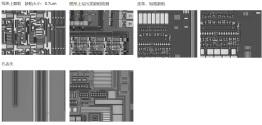
Vip Tornado 3000 adopts a high NA and low magnification optical system, based on UV and multi-band light source system, using different wavelengths for different material layers to achieve the best imaging effect, and the detection algorithm is based on D2D detection mode and automatic dynamic threshold, achieving the best balance between detection rate and pass rate.
TGV glass substrate
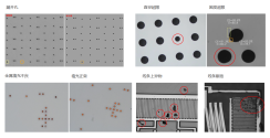
Through-Glass Via (TGV) interconnection technology is derived from 2.5D/3D integrated TSV adapter board technology, which is mainly used to solve the problems of TSV adapter board's degradation of high-frequency or high-speed signal transmission characteristics due to silicon substrate loss, high material cost and complex process. In the TGV process, it mainly consists of steps such as opening holes, filling metals, and making circuits. Corresponding defect detection is required in these processes to ensure the final product yield.
Logic Chip
As the integration of electronic components increases, the demand for testing becomes more stringent. As the core of integrated circuits, the quality of logic chips directly affects the performance of electronic products. Vip's Tornado series products use optical systems and image processing algorithms to achieve efficient and accurate detection of appearance defects in logic chips, ensuring the stability and accuracy of the test results, and becoming a key link in ensuring the quality of logic chips.
The characteristics of logic chips are complex graphics. Dense graphics areas and sparse areas coexist in one DIE. Different layers of film have different materials, and the imaging quality is different for light sources of different wavelengths. At the same time, different thresholds need to be set for rough areas and smooth areas to reduce over-inspection.

Vip Tornado 3000 adopts a high NA and low magnification optical system, based on UV and multi-band light source system, using different wavelengths for different material layers to achieve the best imaging effect, and the detection algorithm is based on D2D detection mode and automatic dynamic threshold, achieving the best balance between detection rate and pass rate.
TGV glass substrate
Through-Glass Via (TGV) interconnection technology is derived from 2.5D/3D integrated TSV adapter board technology, which is mainly used to solve the problems of TSV adapter board's degradation of high-frequency or high-speed signal transmission characteristics due to silicon substrate loss, high material cost and complex process. In the TGV process, it mainly consists of steps such as opening holes, filling metals, and making circuits. Corresponding defect detection is required in these processes to ensure the final product yield.

Major fund projects worth over 130 billion yuan announced, integrated circuits "take the ride"
Recently, major fund projects with a total scale of over 130 billion yuan were officially launched, including the Ningbo AIC Equity Investment Fund Cluster Cooperation Project, the "361" Industrial Fund Cluster Cooperation Project and the "1+N" State-owned Assets and State-owned Enterprises Fund Cluster Cooperation Project.
Among them, the Ningbo "361" industrial fund cluster cooperation project has attracted much attention. It is reported that the "361" industrial fund cluster is a fund cluster jointly established by the Ningbo Municipal Finance Bureau and several investment institutions.
Specifically, Ningbo's "361" industrial fund cluster refers to three trillion-level industrial clusters, including digital industries, green petrochemicals, and high-end equipment; six hundred billion-level industrial clusters, namely new functional materials, new energy, key basic components, smart home appliances, fashionable textiles and clothing, and modern health; a number of emerging and future industrial clusters, mainly involving cutting-edge new materials, future intelligence, metaverse, future energy, aerospace technology, future ocean, quantum technology, original new drugs, and future diagnosis and treatment.
The digital industry cluster involves integrated circuits, optical electronics and sensors, electronic materials, software and the Internet. As one of the core parts of the "361" industrial cluster, Ningbo's integrated circuit industry has been developing rapidly in recent years. According to statistics from the Ningbo Economic and Information Technology Bureau, in 2023, Ningbo's integrated circuit and related industries will achieve a total industrial output value of approximately 54.5 billion yuan, a year-on-year increase of 10.3%, 8 percentage points higher than the growth rate of industrial output value of the "361" industrial cluster. In particular, the growth rate of the special process integrated circuit industry chain is even more gratifying, with an added value of 12.327 billion yuan last year, a year-on-year increase of 15%.
At present, Ningbo has formed a relatively complete full industrial chain system from design, materials, manufacturing, packaging and testing, equipment, and applications, and has gathered design companies such as Ningbo Daxin Semiconductor, manufacturing companies such as SMIC (Ningbo), and material manufacturers such as Jiangfeng Electronics and Anjie Microelectronics.
In addition, a large number of semiconductor projects in Ningbo are also progressing smoothly. For example, the Ningbo Zhongxin Semiconductor Optoelectronics and Power Devices IDM project was recently completed and put into operation. The project plans to build a wafer factory with a driving effect; in addition, the widely-watched Wide Bandgap Semiconductor Materials and Devices Research Institute also welcomed the first batch of core equipment into the factory in early November.
According to the plan, in the future Ningbo will accelerate its progress towards becoming a national characteristic process integrated circuit industry base around the entire industrial chain of "integrated circuit materials and equipment - integrated circuit design - chip manufacturing - packaging and testing - industry applications".
A look at various driver IC that BYD semi division is producing. A lot of new products that will not only benefit its own ePlatform but also allow it to massively replace foreign supply chain.
The National Integrated Circuit Industry Investment Fund has invested in another EDA unicorn company, the fourth this year!
Following the investment in Jiutongfang, Shenzhen Hongxin Micro-Nano and the EDA tool development startup Quanxin Intelligent Manufacturing this year, the National Big Fund recently invested in another EDA unicorn company, Xingxin Technology. The China Semiconductor Industry Association predicts that the scale of China EDA market will reach 18.49 billion yuan in 2025, accounting for 18.1% of the global market.
Industry data shows that compared with the rapidly growing market size, among the hundreds of EDA point tools, my country still has about 40% of the process gaps waiting to be filled by domestic software. The entry of the National Big Fund is expected to further promote the development of the localization of the EDA industry.

Industry data shows that compared with the rapidly growing market size, among the hundreds of EDA point tools, my country still has about 40% of the process gaps waiting to be filled by domestic software. The entry of the National Big Fund is expected to further promote the development of the localization of the EDA industry.

what about cockpit chips ?? this is high end segment and foreign companies dominate. NIO design first 7nm cockpit chip last year and first ADAS chip this year but most probably fabbed by TSMC .. i think manufacturing is the issue in this sector as you need high end chips. SMIC could supply 7nm with enough capacity..
A look at various driver IC that BYD semi division is producing. A lot of new products that will not only benefit its own ePlatform but also allow it to massively replace foreign supply chain.
The article doesn't make sense .CXMT was exempted because of lobbying from Japan as it's almost half of Tokyo Electron's business.@curiouscat could you please link this article to pastebin? It's a great news that CXMT was able to buy more time to expand on its fab and validate domestic equipments but am curious how they managed to do it
Restrictions would have destroyed Tokyo Electron more than CXMT .
do you have a picture of this 7nm chip? I have not seen it.what about cockpit chips ?? this is high end segment and foreign companies dominate. NIO design first 7nm cockpit chip last year and first ADAS chip this year but most probably fabbed by TSMC .. i think manufacturing is the issue in this sector as you need high end chips. SMIC could supply 7nm with enough capacity..
BYD has designed BYD9000.
from hswz zhihu account
She played a vital role in the success of the "Huawei Vibration Reduction" project.
There are hundreds of parts of the shock absorber, large and small. Each part determines success or failure, and each part requires independent research and development. After years of research and development by Chen Xuedong’s team through material preparation, assembly, testing, etc., the vibration absorber technology has been improved from 3% vibration transmission to less than 0.3%, overcoming the problem of “stuck neck” of domestic lithography machine vibration absorbers. The quasi-zero stiffness shock absorber invented has filled the technical gap of domestic high-end active shock absorbers, and has gradually been upgraded to the world's leading level, achieving domestic substitution and supporting production.

