You are using an out of date browser. It may not display this or other websites correctly.
You should upgrade or use an alternative browser.
You should upgrade or use an alternative browser.
Chinese semiconductor thread II
- Thread starter vincent
- Start date
mainland firms will soon outpace Taiwanese ones in DDIC production. Huge change from 2022 when Taiwan had 2 to 1 advantage
Chip war: US exempts some Chinese firms from curbs in concession to Japan, sources say
The US spared China’s top producer of dynamic random-access memory (DRAM) from its latest round of chip export restrictions because of opposition from Japan
missing on that blacklist were some of China’s largest semiconductor companies, including ChangXin Memory Technologies (CXMT). Their absence was partly due to the influence of Japan, whose leading chipmaking tool producer Tokyo Electron is a major supplier to the Chinese firm, according to a person who was briefed on the matter but declined to be named.
Quite surprising if true. Didn't expect Japan to react against US will...and even more surprising didn't expect US to carve in to Japan (this has to be a once in a lifetime event!).
Japan and the Netherlands, both home to the world’s most advanced manufacturers of chipmaking equipment, were exempted in the latest updates to the US Foreign Direct Product Rule, meaning that sanctioned Chinese companies can still buy some chip tools from these countries.
At the moment it is still not clear the real impact of this last round of restrictions on ASML and Japan regarding their sell to China in 2025....we will see.
Meanwhile, equipment made in Malaysia, Singapore, Israel, Taiwan and South Korea is subject to control.
Instead for US manufacturers, because now there is in place the Direct Product Rule (i.e. total ban) for Malaysia and Singapore, where AMAT and LAM assemble tools for China, the immediate future appears bleak.
Regarding entity listing of Chinese SME, for some it will have no impact, for others probably it will have some impact. Anyhow it is a necessary step for Chinese SME to rely on a fully localized supply chain. So now US pushes also the laziest ones to do what they already had to do.
Last edited:
Another one bite the dust, this followed Intel struggles with their 18A project , having trouble with their low yield process rumored to be at 10%. With this I predict 2026 onward we will see an all Chinese line up with TSMC leading the pack followed by SMIC in the leading edge node (2nm for TSMC and 3nm for SMIC)
2 days ago — Samsung has reportedly disbanded a division within its foundry which hints at plans to abandon the company's ambitions for 2 nm chipsets.
Missing:research | Show results with:
4 hours ago — ... 18A Process Rumored to Report Low 10% Yield, Hindering Mass Production ... The lack of yield rates and the struggles with Intel Foundry ...
2 days ago — Samsung has reportedly disbanded a division within its foundry which hints at plans to abandon the company's ambitions for 2 nm chipsets.
Missing:
4 hours ago — ... 18A Process Rumored to Report Low 10% Yield, Hindering Mass Production ... The lack of yield rates and the struggles with Intel Foundry ...
a look on industrial diamond dominance, it's great semi properties and importance in RF applications.
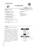
The day after the US announced the semiconductor sanctions, Huawei announced the HBM chip patent. HBM chips are key chips for Al, and the market has long been monopolized by SK Hynix and Samsung. Domestic analysts pointed out that in order to break through the HBM technology threshold, domestic companies first need to produce first-class DRAM, and then develop 3D stacking technology. The technical threshold and manufacturing process requirements of advanced DRAM are extremely high, and it also relies on the support of EUV exposure machines.

Big funds invest in EDA companies
Hangzhou Xingxin Technology Co., Ltd. (hereinafter referred to as Xingxin Technology) has undergone industrial and commercial changes. Yancheng Jiaxiancheng Information Technology Consulting Partnership (Limited Partnership) and Yancheng Qingcheng Investment Partnership (Limited Partnership) have withdrawn from the ranks of shareholders, and the National Integrated Circuit Industry Investment Fund Phase II Co., Ltd., Hangzhou Jiaxiancheng Information Technology Consulting Partnership (Limited Partnership), and Hangzhou Qingcheng Investment Partnership (Limited Partnership) have been added as shareholders. The registered capital has increased from approximately RMB 8.962 million to approximately RMB 9.665 million. At the same time, some key personnel have also changed. The official
website shows that Xingxin Technology has an industry-leading EDA team and core technology. It is an EDA company with completely independent intellectual property rights and international competitiveness. It is committed to developing industry-leading Signoff tool chains, and using breakthrough Signoff technology to fully help customers achieve better power consumption, performance and area (PPA) goals, promote chip design and manufacturing collaboration (DTCO) and enable the development of the global integrated circuit industry.
It is reported that the core team of Xingxin Technology is led by well-known overseas returnee scientists with an average of more than 20 years of rich experience in EDA and chip design. They have led the research and development of many mainstream EDA tools, high-performance computing chips and low-power communication chips in the industry. With the continuous support of industrial chain resources at home and abroad, Xingxin Signoff's overall solution has taken shape. It has been recognized by many top 10 semiconductor companies at home and abroad and has reached a strategic partnership. It has worked together to establish an ecosystem and industrial alliance to help enhance the core competitiveness of the EDA industry.
New MOCVD reactor design promotes innovative development of GaN materials.
The report shows that by optimizing the reactor structure and flow field design, the utilization efficiency of Mo source and reaction gas can be improved, thereby increasing the growth rate of GaN epitaxial layer. Developing new MOCVD experimental equipment with unique features and avoiding homogenized research can improve the level of innovation.
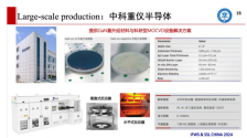
In the gas phase reaction process of the reaction gas, proper pretreatment of the gas source and increasing the space temperature above the substrate play a positive role in suppressing the point defects associated with the yellow band. Adopting the FME mode and optimizing the alternating introduction time of TMAl and NH3 can effectively relieve the mismatch stress in the AlN/AlGaN material and prevent phase separation caused by the component drag effect.
Effective regulation of the temperature gradient in the reactor can induce pre-warping in the substrate, which can be used to compensate for stress in the epitaxial layer. By regulating the V-pit structure in the AlGaN epitaxial layer, the single-layer buffer layer technology is expected to achieve crack-free uniform epitaxial growth of Si-based GaN thick films. The innovative design of the reactor structure and flow field in MOCVD equipment is crucial to the development of related semiconductor material devices.
Zhongke Chongyi Semiconductor Technology Co., Ltd. is a national high-tech enterprise focusing on the production and technology application of third-generation semiconductor gallium nitride (GaN) materials. The company was established in 2021, with its R&D center in Beijing and its production base in Suzhou. The company is mainly engaged in the production and sales of domestic high-end scientific research MOCVD (metal organic chemical vapor deposition) equipment, as well as high-quality, large-size GaN epitaxial wafer materials, and can provide a variety of semiconductor testing, analysis and customized solutions and other services. Related products can be widely used in consumer electronics, renewable energy, data centers, new energy vehicles and other fields.

