Chinese semiconductor thread II

tokenanalyst

Brigadier
Registered Member

Dunyuan Polycore Quartz Crucible: To compete with international leaders​


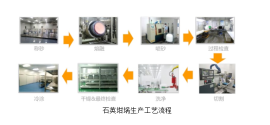
Dunyuan Polycore is one of the few companies in China that can mass-produce large-size semiconductor quartz crucibles. In the field of semiconductor quartz crucibles, the company's technology and products are relatively mature and are continuously iterating. After years of industry precipitation and technology accumulation, it has achieved a leading advantage in the field of semiconductor quartz crucibles in China, and its products have gradually been recognized and used in batches by global leading customers such as GlobalWafers, Siltronic, SK Siltron, Hejing Technology, and Okmetic.
1733505352778.png
Dunyuan Polycore Quartz Crucible Products Dunyuan Juxin can produce both semiconductor quartz crucibles and solar quartz crucibles. Currently, the company mainly produces semiconductor quartz crucibles. The company's quartz crucible products can currently cover semiconductor and solar quartz crucibles in the specification range of 14 inches to 37 inches. The inner diameter, outer diameter, height, wall thickness, etc. of different products vary greatly. Among them, large-size products have higher technical and process difficulties and are the company's main products.

The high-purity semiconductor quartz crucible preparation technology, high-strength quartz crucible preparation technology, and bubble control technology developed by Dunyuan Juxin have been maturely applied in the manufacturing process of the company's semiconductor quartz crucibles (especially large-size) products, and have played an important role in improving the purity, strength and production performance of quartz crucibles.

1733505391389.png

Please, Log in or Register to view URLs content!
 

tokenanalyst

Brigadier
Registered Member

Xinbaite was awarded the qualification of "National High-tech Enterprise" and its innovation drives the upgrading of RF chip industry.​


Recently, the Office of the National High-tech Enterprise Certification Management Leading Group announced the public list of "The Second Batch of High-tech Enterprises in Jiangsu Province in 2024". Xinbaite Microelectronics (Wuxi) Co., Ltd. (hereinafter referred to as "Xinbaite") was successfully selected as a "National High-tech Enterprise" for its core technological advantages and innovative scientific and technological achievements in the field of RF chips. This marks Xinbaite's leading position in the industry and its important role in promoting the development of regional and even national high-tech industries.

The technical team of Xinbaite has worked for many world-leading integrated circuit companies (such as Qualcomm, Qorvo, Skyworks, and Spreadtrum) for many years. These team members not only have a deep background in RF front-end chip R&D, packaging, system integration, sales, and service, but also have excellent design capabilities in various processes such as CMOS/SOI/GaAs/SiGe/GaN and various devices such as PA/LNA/SW/FEM/filter/MEMS.

Since its establishment, Xinbaite has independently developed nearly 50 chips, of which more than 20 chips have been put into mass production. Xinbaite's product lines include WiFi, 5G communications, AIoT, UWB, V2X, etc. The relevant products have been rigorously tested by domestic top communication equipment manufacturers and supplied in batches, and have established a solid strategic cooperative relationship with the upstream and downstream industrial chains of the industry.

The main application markets of Xinbaite's products and services include consumer electronics, communication equipment, medical electronics, automotive electronics, Internet of Things, smart devices, satellite communications, special industries and many other fields.

The company's current product direction is mainly aimed at the next-generation wireless communication protocols. It has leading technology in high-performance (high linearity, high efficiency, high power, high bandwidth) RF power amplifiers, ultra-low noise RF amplifiers, PAMiD integrated filter RF modules, etc. It has applied for and obtained nearly 100 patent licenses for technological innovation, including invention patents, utility model patents, layout patents and software copyrights, which fully demonstrates Xinbaite's deep accumulation in the field of technology and unique innovation capabilities.

Please, Log in or Register to view URLs content!
 

tokenanalyst

Brigadier
Registered Member

New progress has been made in the rapid simulation of large-area mask three-dimensional lithography latent images​


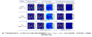
Lithography physical simulation based on the physical model of the lithography process can predict the three-dimensional morphology of the lithography latent image, photoresist exposure, development and other results. Compared with the fast simulation method based on the data fitting model, lithography physical simulation has the advantage of high precision, but its low efficiency makes it difficult to quickly simulate and predict the three-dimensional lithography latent image of the large-area mask structure.

Based on the above problems, the computational lithography team of the EDA Center of the Institute of Microelectronics proposed a method for fast simulation of large-area mask lithography latent images based on deep learning. This method first establishes a three-dimensional latent image database of masks and generates an adversarial network under training conditions. The trained network is used to calculate the three-dimensional latent image of the local position in the large-area mask, and the final result is obtained by splicing. This method avoids the direct calculation of the three-dimensional latent image of the large-area mask and can realize the direct mapping of the mask pattern to the three-dimensional latent image. Simulation experimental data show that compared with the strict solution of the electromagnetic field method, this method has an accuracy of more than 90% and a speed increase of 2.5 to 4.7 times. This achievement improves the efficiency of three-dimensional lithography simulation and expands the application of artificial intelligence-related algorithms in the field of computational lithography.

1733511092079.png

Please, Log in or Register to view URLs content!
 

tokenanalyst

Brigadier
Registered Member

The Institute of Microelectronics has made new progress in the field of SRAM in-memory computing​


Artificial intelligence is widely used in image recognition, audio processing, natural language processing, large models and other fields. Emerging intelligent applications have put forward higher requirements on the computing power and energy efficiency of AI chips. In-memory computing technology can greatly reduce redundant data handling and effectively improve the energy efficiency of AI chips by deeply integrating storage and computing. Among various storage media, SRAM has significant advantages such as low operating voltage, fast read and write speed, low read and write power consumption, and good process compatibility. In recent years, SRAM-based in-memory computing chips have made a qualitative leap in energy efficiency and computing power compared with traditional architectures. Different application scenarios usually require different computing bit widths to achieve the optimization of computing accuracy and energy efficiency. However, the current SRAM-based in-memory computing chips still face problems such as array utilization and energy efficiency loss under different configurations, which makes it difficult to achieve optimal energy efficiency.

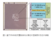
In response to the above problems, the team led by Qiao Shushan, a researcher at the Institute of Microelectronics, Chinese Academy of Sciences, designed a digital reconfigurable in-memory computing chip based on SRAM. The in-memory computing chip adopts a fully digital design, which can ensure accurate calculations under different bit width configurations. In order to achieve high utilization and high energy efficiency under different bit width configurations, the team proposed a digital in-memory computing architecture based on row calculation, which can realize signed/unsigned calculations under any bit width within 1-8 bits, and can achieve extremely high computing resource utilization under different configurations. In order to further improve the energy efficiency of the system, the team designed a low-power summation array with the highest power consumption in the digital in-memory computing chip, proposed a summation array based on a 4-2 compressor, and designed a low-power 4-2 compressor using a customized design method, which effectively reduced the energy consumption of the summation operation. The in-memory computing chip supports a computing bit width of 1-8 bits, and the peak energy efficiency of 1-bit multiplication and accumulation exceeds 2238TOPS/W, and the peak energy efficiency of 4-bit multiplication and accumulation exceeds 44.82TOPS/W.

1733511196941.png
Please, Log in or Register to view URLs content!


tokenanalyst

Brigadier
Registered Member

Researchers develop new polymer semiconductor crosslinker​


Progress has been made in the design and synthesis of high-mobility polymer semiconductors, but it is difficult to apply the unique properties of polymer semiconductors, such as solution processability and intrinsic flexibility, to integrated circuits. In integrated circuits, patterning of polymer semiconductors can reduce leakage current, avoid crosstalk between adjacent devices, and reduce overall circuit power consumption. Currently, controllable photochemical crosslinking technology is a patterning method that is compatible with existing microelectronics industry lithography processes. In particular, the development of efficient chemical crosslinkers is crucial.

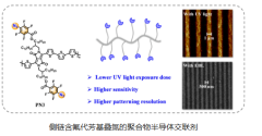
Based on previous results, Zhang Deqing's research group at the Institute of Chemistry, Chinese Academy of Sciences, developed a new polymer semiconductor crosslinker containing fluorinated aromatic azide at the end of the side chain. The study used the commonly used small molecule crosslinker 4Bx as a reference to evaluate the photolithographic patterning performance of PN3 on n-type, p-type and bipolar polymer semiconductors. The study found that PN3 has higher sensitivity than the small molecule crosslinker 4Bx; after PN3 was blended with the three polymer semiconductors, the surface morphology, interchain stacking and mobility of the film were almost unaffected by the patterning process.

Furthermore, the study showed that the photolithography performance of the polymer semiconductor crosslinker was better than that of the small molecule crosslinker. This is because the fluorophenyl azide is evenly distributed at the end of the polymer side chain, and there are multiple crosslinking sites on one polymer molecule; compared with the commonly used small molecule crosslinkers, the polymer semiconductor crosslinker is more evenly dispersed in conventional polymer semiconductor films.

1733511489221.png
 

tokenanalyst

Brigadier
Registered Member

KiloWatt Class Lasers for EUV Lithography, already going commercial.​


The project of "Key Technology and Industrialization of High-Power Thin-Disk Ultrafast Lasers" conforms to the inherent needs of ultra-precision manufacturing development and manufacturing transformation and upgrading, focusing on the key technologies of kilowatt-class solid-state lasers, especially ultrafast lasers, with the goal of quickly realizing the industrialization of high-power thin-disk ultrafast lasers in China. With its advantages of high energy, narrow pulse width, high repetition rate, high peak power and high average power, this laser technology can not only overcome the heat dissipation limitations of the traditional rod-shaped crystal structure technology route, but also avoid the shortcomings of the fiber laser technology route that is not suitable for large pulse energy and high peak power due to laser damage and nonlinearity. It can better realize high-efficiency, high-quality, high-reliability and low-cost precision processing, especially "cold processing", and is suitable for high-end processing scenarios in many fields such as aerospace, semiconductors, new displays, new energy, automobiles, carbon fiber, robots, biomedicine, scientific research, etc. Among them, in the field of ultra-precision machining, the laser can achieve efficient machining, effectively reduce flying chips and burrs, and improve production efficiency; in the semiconductor field, high-energy, high-repetition-rate ultrafast lasers are the core technology supporting EUV light source pre-pulses; in the field of cutting-edge science, thin-film laser technology is an effective means to achieve high-average-power attosecond drive pulses, providing an effective path for attosecond technology to move towards commercial use; in other high-end processing scenarios such as new displays, high-power, large-pulse-energy ultraviolet and deep ultraviolet thin-film lasers will replace the excimer lasers that currently need to be imported with better stability and better costs. It can be seen that thin-film lasers have broad application prospects in many high-end and cutting-edge fields and will support the development of these fields.

Internationally, Germany's TRUMPF has mastered this laser technology and launched a series of products. However, the industrialization of this laser in China is still blank, and the gap with the aforementioned companies is concentrated in key technologies such as the design, manufacturing and packaging process of thin-film laser gain modules and multi-stroke pump modules. As a leading domestic solid-state and ultrafast laser company, has made breakthroughs in many key technologies based on its own profound technical and industrialization accumulation and through years of cooperative research with leading domestic scientific research institutions, and has a solid foundation for promoting industrialization.

This time, has joined hands with leading domestic research institutions such as the Dalian Institute of Chemical Physics, Chinese Academy of Sciences, Zhejiang University, and Shenzhen University to focus on the design, manufacturing and packaging process of thin-disk laser gain modules with completely independent intellectual property rights, multi-stroke pump modules, and high-power picosecond thin-disk laser core components. It will form more innovations and invention patents in design, materials, processing, packaging, and debugging, accelerate the industrialization process of high-power thin-disk ultrafast lasers, and thus support the development of high-end manufacturing.

As one of the "major science and technology special projects", the Shenzhen Science and Technology Innovation Bureau has recently approved the project to fund the company to achieve its expected goals.

The "Key Technology and Industrialization of High-Power Thin-Disk Ultrafast Lasers" project is based on the company's deep technical and industrial accumulation in the field of solid-state and ultrafast lasers. It will achieve a leap from hundreds of watts to thousands of watts for industrial-grade lasers with completely independent intellectual property rights, and open up new and broader application areas with significant performance advantages. The company will take this as an opportunity to uphold innovation-driven development, firmly follow the path of "specialization, precision and innovation", further strengthen its leading edge in the domestic laser industry, enhance its competitiveness in the global laser industry, and fulfill its mission of "using lasers to benefit mankind".​
 
Last edited:
Top