Chinese semiconductor thread II

tokenanalyst

Brigadier
Registered Member

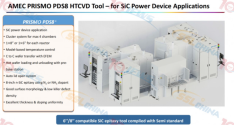
AMEC: PRISMO PDS8 – CVD equipment for epitaxial growth of SiC power devices​


As one of the typical representatives of wide bandgap semiconductor materials, silicon carbide (SiC) has a wide range of applications in high-power, high-frequency fields such as power devices, photovoltaic inverters and electric vehicles. In recent years, the market for silicon carbide power devices has been expanding rapidly, so the demand for larger diameter and higher quality epitaxial layers has become more and more urgent.

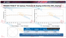
The latest CVD platform for SiC epitaxial growth developed by AMEC, PRISMO PDS8 TM , is compatible with 6- and 8-inch SiC substrates for homogeneous epitaxy. Combining numerical simulation and experimental research, it is proved that the parasitic deposition of gas phase transport and reaction precursors will lead to the redistribution of gas phase components above the wafer surface. By optimizing the process, an epitaxial layer with excellent thickness and doping concentration uniformity, smooth surface and low defect density is quickly grown on a 6-inch 4H-SiC substrate. The epitaxial growth rate exceeds 50 μm/h, and the thickness and doping concentration uniformity are 1.03% and 0.73%, respectively.
1733410468641.png
1733410490102.png

Please, Log in or Register to view URLs content!
 

tokenanalyst

Brigadier
Registered Member

Zhongke Tongzhi's patent for "a wafer bonding machine" was authorized.​


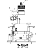
The utility model relates to the technical field of wafer bonding, a wafer bonding machine, comprising a fine-tuning mechanism, a small cylinder assembly, an oil cylinder assembly, a pressure assembly and a vacuum chamber; the fine-tuning mechanism is arranged above the small cylinder assembly and the upper part of the top block of the small cylinder assembly is movably embedded in a groove of the fine-tuning mechanism, the small cylinder assembly is arranged inside the oil cylinder assembly, the lower part of the top block of the small cylinder assembly is fixedly arranged on the upper part of the hydraulic cylinder piston of the oil cylinder assembly, the pressure assembly is arranged below the oil cylinder assembly, the lower part of the hydraulic cylinder piston of the oil cylinder assembly is sealed and fixedly arranged on the weighing sensor of the pressure assembly, and the lower part of the pressure assembly is sealed and fixedly arranged on the upper pressure head of the vacuum chamber, which solves the problems of easy breakage of wafers and low bonding accuracy during wafer bonding.

1733410978409.png

Please, Log in or Register to view URLs content!
 

sunnymaxi

Major
Registered Member

The new production center of Ruili Scientific Instruments was officially put into use, opening a new chapter in mass testing​


Recently, Ruili Scientific Instruments (Shanghai) Co., Ltd. held a launching ceremony for its new production center. The company's latest optical measurement equipment TFX-R3 and optical defect detection equipment BriteSD300 were launched at the launching ceremony. This event marks Ruili's entry into a new stage in the field of semiconductor measurement and testing, and has injected strong momentum into the company's future development.

View attachment 140433

With the rapid expansion of business scale, especially the sharp increase in order volume, Ruili Scientific Instruments (Shanghai) Co., Ltd.'s original clean production site in Heqing has reached saturation. In order to meet this challenge and meet new development needs, the company decided to expand a new production base in Gubo Road Science Park.

In this golden autumn season, the new production center with a total area of 4,000 square meters was officially put into use. Among them, the Class 1,000 clean workshop occupies half of the area, reaching 2,000 square meters. The commissioning of this new center is not only a powerful supplement to the company's current production capacity, but also provides a solid backing for future business growth.

The establishment of the new production center is an important measure for Ruili Scientific Instruments to actively adjust its strategy and expand its production capacity in the face of market challenges. It will greatly enhance the company's production capacity and service quality, ensuring that the company can continue to provide customers with high-quality products and services. The completion of this new position marks that Ruili Scientific Instruments has stepped onto a new level in the field of integrated circuit measurement.

Please, Log in or Register to view URLs content!
Measurement equipment is one the fastest growing sectors right now..

Jingmei Semiconductor

Ruili Scientific Instruments

Yuwei Semi

Hefei Nano Semiconductor Co., Ltd
 

tokenanalyst

Brigadier
Registered Member

Harbin Institute of Technology has made new breakthroughs in the field of silicon carbide integrated photon quantum entanglement devices​


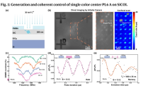
The School of Integrated Circuits at the Shenzhen campus has made important progress in the field of photonic quantum devices. The research results were published in Nature Communications under the title of "Room-temperature waveguide integrated quantum register in a semiconductor photonic platform". The research team successfully prepared the entangled state of a single electron and nuclear spin in a silicon carbide on insulating layer (SiCOI) waveguide, demonstrating the ability to effectively control these spins under room temperature conditions.

1733416424747.png

Please, Log in or Register to view URLs content!


tokenanalyst

Brigadier
Registered Member


Total investment of 3 billion! BOE Qingdao base supporting project is about to start production.​


News came recently from Qingdao Economic and Technological Development Zone that Wanda Optoelectronics Intelligent Manufacturing Base, an important supporting project of BOE Qingdao Base, has successfully passed the completion acceptance and is about to be fully put into production and operation, entering a new stage of development.

The Wanda Optoelectronics Intelligent Manufacturing Production Base Project is located in the Qingdao New Display Industrial Park in the Wangtai area of Qingdao Development Zone. It is invested and constructed by Fujian Wanda Group Co., Ltd. with a total investment of 3 billion yuan. The project mainly builds an optoelectronic intelligent manufacturing base that integrates the design, production and research and development of backlight sources, SMT patches, die-cutting and stamping parts. The first phase of the project plans 12 backlight and SMT patch production lines to provide strong supporting support for BOE's Internet of Things mobile display port device project. At present, the daily production capacity of the 6 SMT production lines that have been built is about 15,000 pieces. The equipment for the second phase of the project has been installed and is in trial operation.

Please, Log in or Register to view URLs content!
 

tokenanalyst

Brigadier
Registered Member
Great job by the clowns stooges in D.C. they harmed US companies to achieve nothing except annoying everyone. As expected.

Huawei's mobile phones have achieved 100% domestic production of all chips, no longer using American chips.​


Huawei's Mate 70 series officially ushered in its first sale. In a conversation with Zhang Quanling, founding partner of Ziniu Fund, He Gang, CEO of Huawei's Terminal BG, made it clear that every chip in the Huawei Mate 70 series has domestic production capabilities, which also means that Huawei's mobile phones have finally achieved 100% domestic production of chips.

Please, Log in or Register to view URLs content!
 

tokenanalyst

Brigadier
Registered Member

Dinglong Co., Ltd.'s CMP polishing pad sales revenue hit a new high in a single quarter!​


Dinglong Co., Ltd. stated in response to investors' questions that the company's CMP polishing pad business achieved product sales revenue of 225 million yuan in the third quarter of 2024, a month-on-month increase of 38% and a year-on-year increase of 90%, setting a new historical single-quarter revenue record.

Chemical mechanical polishing (CMP) is a global flattening process for workpiece surfaces. It is used for polishing micro-nanoscale material surfaces. The basic principle is that the workpiece material surface reacts chemically with the oxidant in the polishing liquid to form a soft layer. Under external pressure, the abrasive particles and the workpiece material surface undergo mechanical grinding to remove the soft layer. Then the workpiece surface reacts chemically again, alternating between chemical and mechanical actions until the workpiece surface is polished.

Please, Log in or Register to view URLs content!
 

tokenanalyst

Brigadier
Registered Member

Domestic EDA releases a new static verification product!.​


Innoda (Chengdu) Electronic Technology Co., Ltd. grandly launches two new static verification EDA tools: EnAltius® CDC cross-domain checking tool and Lint RTL code checking tool . The launch of these two tools will further improve the efficiency and reliability of chip design and promote the development of China's chip industry.

Static verification is to find problems in the design by analyzing the source code of the design. As a commonly used method in the industry, by cooperating with dynamic simulation verification and formal verification in the design, it can significantly improve the coverage of verification, help designers to find and diagnose design defects more quickly in the early stage of design development, and thus shorten the time required for design verification. The release of these two tools further enriches Innoda's product line. So far, Innoda has launched 6 static verification and analysis EDA tools for digital circuits.
  • EnAltius® CDC Cross-Domain Check Tool
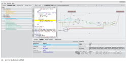
Clock Domain Crossing is a common and complex problem in digital integrated circuit design. Improper clock domain handling usually leads to problems such as metastability, data loss, potential glitches, and loss of multiple data correlation, which can cause abnormal chip functions or even failure, and is one of the main factors for tape-out failure. EnAltius® CDC can provide users with concise violation reports in the shortest time while ensuring the completeness and accuracy of cross-clock domain CDC checks
  • EnAltius® Lint RTL code checking tool
Lint tools are the right-hand man of code engineers. They can find potential syntax errors and logic errors in design codes, especially when IP, modules, etc. are reused in the design, which often leads to inconsistent styles and problems that are not conducive to maintenance. For these problems, the design team must solve them as soon as possible, otherwise they will directly lead to compilation or operation errors, affecting development efficiency and quality. EnAltius®Lint can not only provide basic syntax, semantics and specification checks, but also detect potential defects in the simulation, verification or synthesis stages, helping the design team to achieve "left shift" of checks, thereby achieving early RTL code quality sign-off .

1733436491734.png

Please, Log in or Register to view URLs content!
 

tokenanalyst

Brigadier
Registered Member

Pupil-Shaping Technique in Extreme Ultraviolet Lithography Illumination System​


Abstract

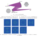
As the critical dimensions of integrated circuits continue to decrease, conventional deep ultraviolet (DUV) lithography machines can no longer satisfy the demand for superior resolution. Currently, extreme ultraviolet (EUV) lithography machines are the most promising for lithography. Generally, an EUV optical system comprises a source, an illumination system, and projection optics. The illumination system, which is located between the source and projection optics, is a key component of an EUV lithography machine. Its primary function is to modulate the spatial and angular spectral distributions of light beam emitted from the source. Simultaneously, it can achieve a uniform illumination of the mask and form multiple illumination modes in the pupil plane. In the early 1990s, scientists attempted to use microoptics devices to shape illumination light (also referred to as pupil shaping), during which the main pupil shaping schemes included diffractive optical elements (DOEs), microlens arrays (MLAs), and micromirror arrays (MMAs). However, when the exposure wavelength is reduced to 13.5 nm, most of the pupil shaping schemes that yield excellent performance in DUV lithography machines are no longer applicable. Currently, the mainstream scheme for pupil shaping in EUV lithography involves the use of double facet mirrors. We can achieve pupil shaping without light loss by changing the facetmapping relationship; additionally, the light emitted from the intermediate focus can offer uniform illumination on the mask. Obtaining a facetmapping relationship is a core issue in pupil shaping. In this study, we investigate the pupil shaping technique of EUV lithography and present an algorithm that can rapidly determine the facet mapping relationship to provide a reference for studies pertaining to EUV pupil shaping techniques.

1733442095075.png

Please, Log in or Register to view URLs content!
 
Top