China has most of these things covered...Lithography is the critical equipment in Wafer fabrication but is totally useless with the rest of the tools, Ok, you bought the ASML NXT-2100, now you need coating-developing tools that can deposit photo resist with good uniformity, deposition tools for the different materials with enough uniformity and throughput, furnaces for oxidation and ion implanters for doping, RPT tools to annealing, Chemical Mechanical Polishers for wafers without damaging the made structures, etching tools that can handled the High Aspect Ratios of modern transistor, precision cleaning tools, metrology tools for yield monitoring, overlay metrology and CDSEM.
And then you have to take into account the materials like photo-resists, gases, liquids and their delivery subsystems, vibration isolation for the lithography machine. the lithography machines is useless without good photoresist, more useless without good overlay metrology and even more useless without good etching tools. And every single of those tools need their subsystems like RF-Matching Networks and maglev pumps.
Only thinking in the lithography machine is the trap that a lot pundits fall into.
You are using an out of date browser. It may not display this or other websites correctly.
You should upgrade or use an alternative browser.
You should upgrade or use an alternative browser.
Chinese semiconductor thread II
- Thread starter vincent
- Start date
This new DUV machine announced by the MIIT. What type of chips can it produce? To me it is of huge value regardless of the number of patterns and low yields. If it can produce Kirin 9010 series types chips even at lower yields than what SMIC can presently do, it matters not. China has the economies of scale to produce the DUV machine en masse.
MIIT was talking about 65nm dry machine ..This new DUV machine announced by the MIIT. What type of chips can it produce? To me it is of huge value regardless of the number of patterns and low yields. If it can produce Kirin 9010 series types chips even at lower yields than what SMIC can presently do, it matters not. China has the economies of scale to produce the DUV machine en masse.
The ArF dry scanner is probably for a 65nm planar process maybe 45 nm with double patterning or could be use for the interconnect layers of immersion scanners patterned ICs.This new DUV machine announced by the MIIT. What type of chips can it produce? To me it is of huge value regardless of the number of patterns and low yields. If it can produce Kirin 9010 series types chips even at lower yields than what SMIC can presently do, it matters not. China has the economies of scale to produce the DUV machine en masse.
the KrF scanner looks like is mainly 180 to 70 nm <if they use the overlay system of the ArF scanner>. Judging by the below 25nm overlay it seems that costumers of this KrF scanners are looking to use it for patenting the less critical interconnect layers at a pretty low cost.
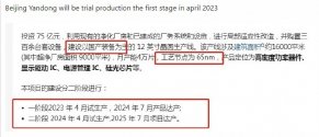
I posted a while back that Yandong semiconductor is first company to use that 65nm DRY DUV for mass production.
They have established a full domestic equipment for that line in April, 2023 for trial production. No much attention is being paid to this because everyone is focusing on SMEE's 28nm scanner.
燕东微使用募集资金投资“基于成套国产装备的特色工艺12英寸集成电路生产线项目”,由全资子公司北京燕东微电子科技有限公司实施,项目总投资75亿元,目标为月产能4万片,工艺节点为65nm,产品定位为高密度功率器件、显示驱动 IC、电源管理 IC、硅光芯片等。
该项目周期的一阶段为2023年4月试生产,2024年7月产品达产;二阶段为2024年4月试生产,2025年7月项目达产。
I posted a while back that Yandong semiconductor is first company to use that 65nm DRY DUV for mass production.
They have established a full domestic equipment for that line in April, 2023 for trial production. No much attention is being paid to this because everyone is focusing on SMEE's 28nm scanner.
燕东微使用募集资金投资“基于成套国产装备的特色工艺12英寸集成电路生产线项目”,由全资子公司北京燕东微电子科技有限公司实施,项目总投资75亿元,目标为月产能4万片,工艺节点为65nm,产品定位为高密度功率器件、显示驱动 IC、电源管理 IC、硅光芯片等。
该项目周期的一阶段为2023年4月试生产,2024年7月产品达产;二阶段为2024年4月试生产,2025年7月项目达产。

----------------------------------------------------------------------------------------------------------------------------------
let me clear one very important point ..
MIIT clearly announced 65nm DUV. it means next generation Lithography conquered too.. 28nm immersion..
if anyone follow Chinese high tech industry this is the pattern China always follow. they don't display/publicly announced technology unless next gen tech is near completion or completed. we have countless examples
Media prohibited to take closer shot of WS-10C Engine until 2022 Air show. they not only allowed to take closer shot but J-20 did catwalk in front of audience for the very first time .. and in March 2023, AECC announced WS-15 entered in LRIP stage.. type 094 SSBN interiors pics made public for the first time..
Last edited:
????I posted a while back that Yandong semiconductor is first company to use that 65nm DRY DUV for mass production.
They have established a full domestic equipment for that line in April, 2023 for trial production. No much attention is being paid to this because everyone is focusing on SMEE's 28nm scanner.
燕东微使用募集资金投资“基于成套国产装备的特色工艺12英寸集成电路生产线项目”,由全资子公司北京燕东微电子科技有限公司实施,项目总投资75亿元,目标为月产能4万片,工艺节点为65nm,产品定位为高密度功率器件、显示驱动 IC、电源管理 IC、硅光芯片等。
该项目周期的一阶段为2023年4月试生产,2024年7月产品达产;二阶段为2024年4月试生产,2025年7月项目达产。
This fab has been discussed extensively in the version 1 of this thread.
Havok himself basically said this was the first fab to really use it for mass production.
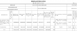
Let's see where are they at from mid year report

Looks like this 12-inch production line is in line with expectations based on what they said here with no changes. They put in another 3B RMB here.
Not much more than that I'm afraid, like yield and such
feel free to check their stock discussion.
if you read MIT( Ministry of Information Technology) recent report.. they clearly mentioned about immersion(28nm) Non-litho tools being reached at international level or even better in some category..
All Non-Litho tools , material and EDA have successfully developed and entered in serial production.. Finfet capable Photoresists also start mass production..
i m not giving any specific date.. but China will be 100 percent self-sufficient in semi supply chain way before than 2035 ..
Technically self-sufficient, sure. But imports are still needed to supply all the demand from fab expansions. Ramping up domestic production is the key.
I was like ??? when reading the article, because I thought China was on the verge of 22/28nm machineView attachment 135948
----------------------------------------------------------------------------------------------------------------------------------
let me clear one very important point ..
MIIT clearly announced 65nm DUV. it means next generation Lithography conquered too.. 28nm immersion..
if anyone follow Chinese high tech industry this is the pattern China always follow. they don't display/publicly announced technology unless next gen tech is near completion or completed. we have countless examples
Media prohibited to take closer shot of WS-10C Engine until 2022 Air show. they not only allowed to take closer shot but J-20 did catwalk in front of audience for the very first time .. and in March 2023, AECC announced WS-15 entered in LRIP stage.. type 094 SSBN interiors pics made public for the first time..


