It's the same drivel that was seen in the last two years. After actuallly reading it instead of just doing a bare skim the article doesn't say anything worth listening to.View attachment 131231
Of course no. That would imply spending money.
From my point of view looks like this guys write their conclusion first <sanctions good because we say so> and then they use Chinese technical bloggers and social media information to write articles obfuscating things.
You are using an out of date browser. It may not display this or other websites correctly.
You should upgrade or use an alternative browser.
You should upgrade or use an alternative browser.
Chinese semiconductor thread II
- Thread starter vincent
- Start date
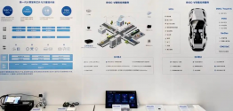
Eswin Computing helps accelerate the development of intelligent connected vehicles
In order to promote the exchange and cooperation of intelligent connected vehicle technology and accelerate the cross-border integration and development of intelligent connected vehicles, the 11th International Intelligent Connected Vehicle Technology Conference (CICV 2024) was held in Beijing from June 18 to 20. The conference invited government departments, enterprises, universities and research institutions, industry organizations, local representatives, and investment institutions in related fields such as automobiles, transportation, and information and communications to participate in the conference to deeply discuss hot and difficult topics in intelligent connected vehicle technology innovation, industrial application, and ecological construction.
Eswi Computing was invited to participate in the conference. Focusing on RISC-V applications in roadside and in-vehicle applications, it exhibited a variety of products and solutions based on RISC-V architecture, including edge computing SoC, in-vehicle MCU, in-vehicle touch chip, touch and display driver integrated chip, electronic rearview mirror SoC, and in-vehicle display power management chip, showcasing the innovative achievements of smart connected vehicles.
DJEL: the key to the advancement of integrated circuit manufacturing process is the accelerated rise of domestic electron beam measurement equipment
Some domestic companies have begun to get involved in this field and have achieved some remarkable results. For example, the electron beam defect detection equipment EBI and key dimension measurement equipment CD-SEM launched by Dongfang Jingyuan were the first to fill the domestic gap. As one of the earliest domestic companies to deploy in this field, its product diversification and product maturity are at the forefront. Testing companies such as Jingce Electronics have also deployed in the electron beam detection market, and some products have been delivered. Given the importance of electron beam quantity detection equipment and extremely high technical barriers, its localization process is of great significance to the independent control of integrated circuit manufacturing.
Dongfang Jingyuan's EBI equipment has passed the 28nm and above process logic verification in June 2021 and entered fully automatic mass production, becoming the first set of equipment in China to complete this verification; in terms of CD-SEM, the 12-inch CD-SEM was launched in June 2021, the 8-inch CD-SEM was launched in March 2022, and the 6&8-inch compatible CD-SEM was launched in April 2023, and dozens of devices have been sold.
From EBI to DR-SEM, accurate measurement leads to progress
The SEpA-i505, which was successfully developed and launched by Oriental Jingyuan as early as 2019, is the first electron beam defect detection equipment in China. It can provide a complete nano-level defect detection and analysis solution, and will enter fully automatic mass production on the 28nm production line in 2021. After several years of research and development iterations, the new generation model SEpA-i525 has been further expanded in terms of detection capabilities and application scenarios. In terms of detection rate, the new EBI product is compatible with step-by-step and continuous scanning. The continuous scanning mode is suitable for Memory Fab. Combined with the performance optimization of the self-developed detector, it can bring 3-5 times the speed improvement compared to the previous generation of models; the newly developed electron optical system design can support negative mode detection methods and detection beam currents of more than 40nA; at the same time, a variety of wafer charging control solutions are introduced to reduce the impact of charging effects on images. In terms of application scenarios, Oriental Jingyuan's EBI equipment has also extended from the logic Fab field to the Memory Fab, which can solve more process defect problems for customers.
In addition, the EBI equipment of Dongfang Jingyuan is based on the DNA defect detection engine, adopts low coupling between the front-end and the back-end, and supports synchronous online/offline inspection. It integrates a variety of advanced defect detection algorithms (D2D, C2C, etc.), which can meet the different application needs of users, effectively improve the capture rate, and reduce the nuisance rate. The automatic defect classification (ADC) engine adopted, in which the Model-Based ADC module is based on deep learning, automatic feature selection, and clustering algorithm with fusion confidence, can effectively improve the Purity and Accuracy of automatic defect classification; the Rule-Based ADC module retains the flexibility of manual experience and can be quickly created in small sample scenarios.
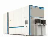
(2) CD-SEM: Comprehensive layout for 6, 8, and 12-inch production lines. CD-SEM (critical dimension measurement equipment) mainly monitors the size of the graphics formed after the photolithography process during the IC manufacturing process by sampling and measuring the critical dimensions to ensure the yield. Oriental Jingyuan's CD-SEM is divided into two product series: 12-inch and 6&8-inch compatible. Both have entered user production lines and can support multiple measurement scenarios such as Line/Space, Hole/Elliptic, LER/LWR, etc., to meet a variety of imaging needs.
After two years of iteration, the new generation of 12-inch CD-SEM model SEpA-c430 has achieved comprehensive improvements in measurement performance and speed, and has been verified on-site at multiple customers. The measurement repeatability of this product reaches 0.25nm, meeting the needs of 28nm production lines; by improving electron beam scanning and signal detection, the production capacity is increased by 30%; the newly launched wafer surface charge compensation function can improve the ability to measure photoresist. The new model also adds an automatic calibration function to ensure high measurement consistency, preparing for large-scale mass production of the product.
It is worth mentioning that Oriental Jingyuan's ODAS LAMP product has been officially released at the end of 2022. The full name of ODAS LAMP is Offline Data Analysis System, Large Scale Automatic Measurement Purpose product, and its Chinese name is Large Scale CD Measurement Offline Data Processing System.
ODAS LAMP is a tool for CD-SEM measurement equipment. It is designed to facilitate CD-SEM users to create and modify CD-SEM recipes offline using design layouts. It also provides a review function for CD-SEM measurement results and can also perform offline re-measurement on CD-SEM images to improve machine utilization.
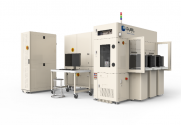
(3) DR-SEM: Targeting new demands and exploring new areas. DR-SEM (electron beam defect re-inspection equipment) is the latest segment that Oriental Jingyuan has entered. According to SEMI data, the demand for DR-SEM for 12-inch production lines in 2024 will be about 50 units. In the next 3-4 years, the total demand for DR-SEM equipment for 12-inch production lines will be about 150 units. According to data from the China Business Industry Research Institute, the demand for DR-SEM in 2024 will be about US$149.1 million, and the demand for DR-SEM equipment in the next 3-4 years will be about US$447 million. In 2023, Oriental Jingyuan launched its first SEpA-r600 TM system, which has been shipped to several leading customers for production line verification. During the equipment development process, thanks to the company's early technical accumulation, such as borrowing from the mature EBI technology, the development process was significantly shortened, and the image quality met customer needs, with CR>95%, close to the level of mature machines.
In the selection of research and development solutions for auxiliary optical system review OM, Oriental Crystal Source bypassed the restrictions of foreign supply chains and independently developed a new optical window imaging system. With the help of this system, the development of optical review function for unpatterned wafers has been completed, and the function of auto bare wafer review has been realized to meet customers' review needs for defects around 70nm. In other words, Oriental Crystal Source's DR-SEM equipment can not only perform pattern wafer auto review, but also unpattern wafer review function, and also provide defect element analysis.
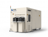
The combination of software and hardware protects chip yield, and domestic substitution is gradually accelerating
Oriental Jingyuan also launched the yield management system software YieldBook. This is a set of industrial software for data integration and analysis throughout the entire life cycle of the chip. YieldBook collects all kinds of data from design, manufacturing, packaging, and testing to establish a unified data platform. Based on this platform, it can conduct individual process quality monitoring, overall defect rate statistics, yield loss traceability analysis, feedback manufacturing difficulties to upstream design, etc., comprehensively monitor factors affecting yield and assist in yield improvement. If the measurement and testing equipment is compared to a "point", then the yield management system is a "line" that connects many points and manages them systematically. It is reported that YieldBook is the first yield management system in the industry to achieve a comprehensive unification of measurement data (MMS), defect data (DMS), and yield data (YMS), breaking the monopoly of international manufacturers, and using the advantages of its own measurement and testing machines to achieve visual management of Fab data. The relevant person in charge of Oriental Jingyuan said: In the future, we will continue to deepen our efforts, while ensuring that the functions are more complete, providing more competitive prices, and more effectively helping customers achieve rapid machine cross-machine and process optimization. In addition, YieldBook will also provide favorable support for the yield management of advanced node chip manufacturing, reducing costs and increasing efficiency while achieving rapid yield growth and stable mass production.
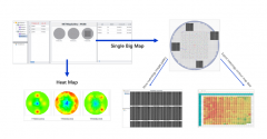
In addition to the above products, Dongfang Jingyuan also has computational lithography software OPC products. It is the only company in China that integrates OPC and detection and measurement equipment.
Dongfang Jingyuan's EBI equipment has passed the 28nm and above process logic verification in June 2021 and entered fully automatic mass production, becoming the first set of equipment in China to complete this verification; in terms of CD-SEM, the 12-inch CD-SEM was launched in June 2021, the 8-inch CD-SEM was launched in March 2022, and the 6&8-inch compatible CD-SEM was launched in April 2023, and dozens of devices have been sold.
From EBI to DR-SEM, accurate measurement leads to progress
The SEpA-i505, which was successfully developed and launched by Oriental Jingyuan as early as 2019, is the first electron beam defect detection equipment in China. It can provide a complete nano-level defect detection and analysis solution, and will enter fully automatic mass production on the 28nm production line in 2021. After several years of research and development iterations, the new generation model SEpA-i525 has been further expanded in terms of detection capabilities and application scenarios. In terms of detection rate, the new EBI product is compatible with step-by-step and continuous scanning. The continuous scanning mode is suitable for Memory Fab. Combined with the performance optimization of the self-developed detector, it can bring 3-5 times the speed improvement compared to the previous generation of models; the newly developed electron optical system design can support negative mode detection methods and detection beam currents of more than 40nA; at the same time, a variety of wafer charging control solutions are introduced to reduce the impact of charging effects on images. In terms of application scenarios, Oriental Jingyuan's EBI equipment has also extended from the logic Fab field to the Memory Fab, which can solve more process defect problems for customers.
In addition, the EBI equipment of Dongfang Jingyuan is based on the DNA defect detection engine, adopts low coupling between the front-end and the back-end, and supports synchronous online/offline inspection. It integrates a variety of advanced defect detection algorithms (D2D, C2C, etc.), which can meet the different application needs of users, effectively improve the capture rate, and reduce the nuisance rate. The automatic defect classification (ADC) engine adopted, in which the Model-Based ADC module is based on deep learning, automatic feature selection, and clustering algorithm with fusion confidence, can effectively improve the Purity and Accuracy of automatic defect classification; the Rule-Based ADC module retains the flexibility of manual experience and can be quickly created in small sample scenarios.

(2) CD-SEM: Comprehensive layout for 6, 8, and 12-inch production lines. CD-SEM (critical dimension measurement equipment) mainly monitors the size of the graphics formed after the photolithography process during the IC manufacturing process by sampling and measuring the critical dimensions to ensure the yield. Oriental Jingyuan's CD-SEM is divided into two product series: 12-inch and 6&8-inch compatible. Both have entered user production lines and can support multiple measurement scenarios such as Line/Space, Hole/Elliptic, LER/LWR, etc., to meet a variety of imaging needs.
After two years of iteration, the new generation of 12-inch CD-SEM model SEpA-c430 has achieved comprehensive improvements in measurement performance and speed, and has been verified on-site at multiple customers. The measurement repeatability of this product reaches 0.25nm, meeting the needs of 28nm production lines; by improving electron beam scanning and signal detection, the production capacity is increased by 30%; the newly launched wafer surface charge compensation function can improve the ability to measure photoresist. The new model also adds an automatic calibration function to ensure high measurement consistency, preparing for large-scale mass production of the product.
It is worth mentioning that Oriental Jingyuan's ODAS LAMP product has been officially released at the end of 2022. The full name of ODAS LAMP is Offline Data Analysis System, Large Scale Automatic Measurement Purpose product, and its Chinese name is Large Scale CD Measurement Offline Data Processing System.
ODAS LAMP is a tool for CD-SEM measurement equipment. It is designed to facilitate CD-SEM users to create and modify CD-SEM recipes offline using design layouts. It also provides a review function for CD-SEM measurement results and can also perform offline re-measurement on CD-SEM images to improve machine utilization.

(3) DR-SEM: Targeting new demands and exploring new areas. DR-SEM (electron beam defect re-inspection equipment) is the latest segment that Oriental Jingyuan has entered. According to SEMI data, the demand for DR-SEM for 12-inch production lines in 2024 will be about 50 units. In the next 3-4 years, the total demand for DR-SEM equipment for 12-inch production lines will be about 150 units. According to data from the China Business Industry Research Institute, the demand for DR-SEM in 2024 will be about US$149.1 million, and the demand for DR-SEM equipment in the next 3-4 years will be about US$447 million. In 2023, Oriental Jingyuan launched its first SEpA-r600 TM system, which has been shipped to several leading customers for production line verification. During the equipment development process, thanks to the company's early technical accumulation, such as borrowing from the mature EBI technology, the development process was significantly shortened, and the image quality met customer needs, with CR>95%, close to the level of mature machines.
In the selection of research and development solutions for auxiliary optical system review OM, Oriental Crystal Source bypassed the restrictions of foreign supply chains and independently developed a new optical window imaging system. With the help of this system, the development of optical review function for unpatterned wafers has been completed, and the function of auto bare wafer review has been realized to meet customers' review needs for defects around 70nm. In other words, Oriental Crystal Source's DR-SEM equipment can not only perform pattern wafer auto review, but also unpattern wafer review function, and also provide defect element analysis.

The combination of software and hardware protects chip yield, and domestic substitution is gradually accelerating
Oriental Jingyuan also launched the yield management system software YieldBook. This is a set of industrial software for data integration and analysis throughout the entire life cycle of the chip. YieldBook collects all kinds of data from design, manufacturing, packaging, and testing to establish a unified data platform. Based on this platform, it can conduct individual process quality monitoring, overall defect rate statistics, yield loss traceability analysis, feedback manufacturing difficulties to upstream design, etc., comprehensively monitor factors affecting yield and assist in yield improvement. If the measurement and testing equipment is compared to a "point", then the yield management system is a "line" that connects many points and manages them systematically. It is reported that YieldBook is the first yield management system in the industry to achieve a comprehensive unification of measurement data (MMS), defect data (DMS), and yield data (YMS), breaking the monopoly of international manufacturers, and using the advantages of its own measurement and testing machines to achieve visual management of Fab data. The relevant person in charge of Oriental Jingyuan said: In the future, we will continue to deepen our efforts, while ensuring that the functions are more complete, providing more competitive prices, and more effectively helping customers achieve rapid machine cross-machine and process optimization. In addition, YieldBook will also provide favorable support for the yield management of advanced node chip manufacturing, reducing costs and increasing efficiency while achieving rapid yield growth and stable mass production.

In addition to the above products, Dongfang Jingyuan also has computational lithography software OPC products. It is the only company in China that integrates OPC and detection and measurement equipment.
TuoJing Technology's product process development and verification progress smoothly, which will promote the expansion of hybrid bonding equipment customers
In 2023, Tuojing Technology launched two new equipment platforms and two new reaction chambers. The design of the new equipment platform further improved the equipment production capacity, and the mechanical production capacity can be increased by about 20% to 60%. The new reaction chamber has improved the performance indicators of thin film deposition.It is understood that the company received more than 130 new reaction chambers from customers last year, and more than 40 new reaction chambers were shipped to customers for verification.
The verification time required for thin film deposition equipment on the wafer fab production line is generally long. According to historical experience, the average verification cycle for mature products is usually around 3-6 months, and the average verification cycle for new products is generally around 6-24 months.Regarding other new products,
Lv Guangquan stated at the performance meeting that the company's product and process development and verification have been progressing smoothly since the first quarter of 2024. "This year, the company will continue to promote customer expansion for hybrid bonding equipment products, gradually gain a deeper understanding of market demand, and further explore applications in more fields such as memory chips, image sensors, and advanced packaging."
ALD and ALE for OptoElectronics, Photonics ,VCSEL, semiconductors ,Gratings and so on.
Guangchi Semiconductor (Optorun) Atomic Layer Coating and Etching Coating Project Completed
Recently, the atomic layer coating and etching equipment project invested and constructed by Opto-Chi Semiconductor Technology (Shanghai) Co., Ltd. successfully completed the final acceptance.
The atomic layer coating and etching equipment project is located in the 07-17 plot of Baoshan Hi-tech Zone, with a total investment of 548 million yuan, covering an area of 50 mu and a total construction area of 64,400 square meters, of which the first phase has a construction area of about 38,000 square meters, covering standard factory buildings, R&D office buildings, etc. The project is mainly committed to the manufacturing of new electronic components and equipment, and utilizes the adjustment of the global pan-semiconductor industry chain and the investment and technology integration of related cutting-edge R&D to realize the industrialization and scale of electronic special equipment manufacturing.
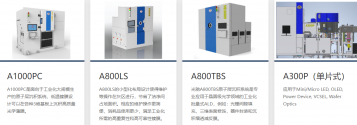
Guangchi Semiconductor Technology (Shanghai) Co., Ltd., as a wholly-owned subsidiary of Guangchi Technology (Shanghai) Co., Ltd., the completion of the project marks that the company will enter the fast lane of development and growth. Since Guangchi Technology settled in the Southern Park in 2000, its product technology market share and competitiveness have continued to expand with its focus and innovation in the field of semiconductor optics. In 2022, Guangchi Technology will integrate traditional optics and semiconductor technology, invest in the establishment of Guangchi Semiconductor in the Northern Park, further increase manufacturing space and production capacity, and open up a new market for the transformation of optical components to semiconductor integrated optics. After reaching full production, the project is expected to have an annual production capacity of 120 high-precision atomic layer coaters and 5 etching machines, becoming an emerging force to help regional industrial upgrading.
Silan Jihong 8-inch silicon carbide power device chip manufacturing production line project started: total investment of 12 billion yuan, first phase trial production in the fourth quarter of next year
This morning (June 18), Silan Jihong's 8-inch silicon carbide power device chip manufacturing production line project started construction in Haicang.
Cui Yonghui, secretary of the municipal party committee, announced the start of the project, and Huang Wenhui, deputy secretary of the municipal party committee and mayor, Chen Xiangdong, chairman of Silan Microelectronics Co., Ltd., and Wu Ling, chairman of the Third Generation Semiconductor Industry Technology Innovation Strategic Alliance, delivered speeches respectively. Municipal leaders You Wenchang and Huang Xiaozhou attended the opening ceremony.
The total investment of the Silan Jihong 8-inch silicon carbide power device chip manufacturing production line project is 12 billion yuan. It will be built in two phases. After completion, it will form an annual production capacity of 720,000 8-inch silicon carbide power device chips. Among them, the total investment of the first phase of the project is 7 billion yuan. It is expected to be initially put into operation at the end of the third quarter of 2025, and trial production will be carried out in the fourth quarter of 2025. After reaching full production, it will produce 420,000 pieces per year. After completion, the project will greatly enhance Silan Micro's silicon carbide chip manufacturing capabilities, better meet the demand for silicon carbide chips required by domestic new energy vehicles, and have the ability to provide high-performance silicon carbide chips for power inverter products such as photovoltaics, energy storage, and charging piles.
Distortion measurement of a lithography projection lens based on multichannel grating lateral shearing interferometry.
Shanghai Institute of Optics and Fine Mechanics, Chinese Academy of Sciences.Center of Materials Science and Optoelectronics Engineering, University of Chinese Academy of Sciences.
State Key Laboratory of Extreme Photonics and Instrumentation, Zhejiang University.
Abstract
The optical distortion of the lithographic projection lens can reduce imaging quality and cause overlay errors in lithography, thus preventing the miniaturization of printed patterns. In this paper, we propose a technique to measure the optical distortion of a lithographic projection lens by sensing the wavefront aberrations of the lens. A multichannel dual-grating lateral shearing interferometer is used to measure the wavefront aberrations at several field points in the pupil plane simultaneously. Then, the distortion at these field points is derived according to the proportional relationship between the Z2Z2 and Z3Z3 Zernike terms (the tilt terms) and the image position shifts. Without the need for additional devices, our approach can simultaneously retrieve both the wavefront aberrations and the image distortion information. Consequently, it improves not only measurement speed and accuracy but also enables accounting for displacement stage positioning error. Experiments were conducted on a lithographic projection lens with a numerical aperture of 0.57 to verify the feasibility of the proposed method.
The new DUV design is roughly equivalent to an original chip that could process a 28nm process in a single pass. Now it can achieve a 14nm process. The four-fold exposure can be improved to an equivalent 1.4nm process and... it can handle 310 wafers/hRumors: Looks like 2nd generation DUV and EUV will be available in 2025-2026
Well, ASML DUV (with the best expertise in Lithography Machine) can do 5nm at best. How can SMEE Lithography can do 1.4nm?The new DUV design is roughly equivalent to an original chip that could process a 28nm process in a single pass. Now it can achieve a 14nm process. The four-fold exposure can be improved to an equivalent 1.4nm process and... it can handle 310 wafers/h
