
You are using an out of date browser. It may not display this or other websites correctly.
You should upgrade or use an alternative browser.
You should upgrade or use an alternative browser.
Chinese semiconductor thread II
- Thread starter vincent
- Start date

Highest efficiency: more than 15 pieces per hour! This ultra-high efficiency equipment from HGLASER helps accelerate the development of the third-generation compound semiconductor industry
Laser annealing, a new generation of key technology
Silicon carbide is a typical representative of the third generation of semiconductor materials. With its excellent physical and chemical properties, it has become a new favorite material in cutting-edge technology fields such as 5G, new energy, AI artificial intelligence, and the Internet of Things. With the advancement of technology and the upgrading of applications, the requirements for annealing processes in semiconductor device manufacturing are constantly increasing. The traditional high-temperature thermal annealing process has various shortcomings. The industry needs a new annealing solution with adjustable area and controllable depth.
The principle of laser annealing is to use a high-energy laser beam, after spot shaping, to irradiate the entire SiC wafer back gold (Ni or Ti layer) to produce an alloying reaction and generate a Si alloy compound layer, a carbon aggregation layer and a carbon vacancy layer, thereby reducing the barrier difference between the transition metal and the SiC substrate, forming a good ohmic contact, and playing a role in reducing contact resistance and improving the electrical performance of the device.
HGLASER, a pioneer in compound semiconductor processing
Faced with the urgent needs of the development of the compound semiconductor market, HGLASER targets the pain points of silicon carbide device processing and focuses on the laser micro-nano processing and measurement of compound semiconductors such as SiC, GaN, InP, and AsGa. Relying on advanced laser processing technology and core technologies such as AOI detection, it comprehensively deploys key processes in the upstream, midstream and downstream of compound semiconductor production, and customizes one-stop system solutions for industry customers.
Fully automatic wafer laser annealing intelligent equipment

It is compatible with 6/8-inch, thinned wafers, bonded wafers and other types of SiC wafer processing. Through the relative movement of the customized laser annealing head and the precision motion platform, the back gold (Ni or Ti layer) of the entire SiC wafer can be annealed to form a good ohmic contact, reduce contact resistance and improve the electrical performance of the device.
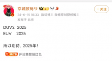
duv version 2,euv in year 2025
Attachments
-
 468E95E9761EABD306A56C36A25026ED.png60.5 KB · Views: 143
bro can't wait for the mythical SSA900A 22nm to be acknowledged in 2025.duv version 2,euv in year 2025
") Major improvement from the basic SSA800A will be an improved MMO, optics and a more powerful power source.
Major improvement from the basic SSA800A will be an improved MMO, optics and a more powerful power source.Changjing Pulian's annual production of 20 billion new components project is expected to be completed and accepted in August
Pukou released news that the major project in Jiangsu Province, Changjing Pulian, has made new progress in its annual production of 20 billion new components. The project has applied for building completion surveying and mapping, and pipeline construction is underway on site. It is expected to complete the completion acceptance by the end of August and be put into operation in September.
It is reported that the Changjing Pulian project with an annual output of 20 billion new components is located in Pukou Economic Development Zone and is invested and constructed by Jiangsu Changjing Pulian Power Semiconductor Co., Ltd. The project covers a total area of 148 mu, with a total construction area of about 129,000 square meters. It will build production plants, power centers, warehouses, etc., and mainly produce surface-mounted semiconductor discrete devices and power devices. After completion and production, it is expected to produce 20 billion devices annually. The annual output value is expected to be 1.2 billion yuan and the annual tax revenue is 50 million yuan.
A quartzite mine survey project in Suichuan, Jiangxi Province passed the acceptance!
Recently, the quartzite mine survey project for Macao glass in Suichuan County, Jiangxi Province, undertaken by the Jiangxi Institute of Geological Exploration, passed the field acceptance organized by the Jiangxi Mineral Resources Security Service Center. The field work of the project started on April 10, 2023 and ended on January 31, 2024. A total of 3.27 square kilometers of 1:10,000 geological surveys, 2,394 cubic meters of trenching, and 781.50 meters of drilling were completed, achieving good prospecting results.
Total investment of 300 million yuan! A quartz sand project in Inner Mongolia is under construction
It is reported that the Inner Mongolia Wanxing Silicon Industry Co., Ltd. is in full swing with a project to produce 300,000 tons per year, and is expected to be put into operation in August. The project mainly produces quartz sand for building panels, with a total investment of 300 million yuan and a total construction area of about 40,000 square meters. It is carried out in two phases, of which the construction of the first phase is nearing completion, and the second phase is in the stage of handling pre-construction procedures. After the first phase is put into operation, the annual output value can reach 300 million yuan, and the profit and tax can reach 15 million yuan.
Annual output of 6,000 tons! Guangxi plans to invest in ultra-high purity quartz sand project for solar photovoltaic
Recently, the Administrative Approval Bureau of Nanning Economic Development Zone in Guangxi approved the environmental impact assessment document of the production base of ultra-high purity quartz sand for solar photovoltaic with an annual output of 6,000 tons by Guangxi Jingpai Silicon-based New Materials Co., Ltd. The total investment of the production base of ultra-high purity quartz sand for solar photovoltaic with an annual output of 6,000 tons by Guangxi Jingpai Silicon-based New Materials Co., Ltd. is 120 million yuan, with a total land area of 10,324 m2. Two ultra-high purity quartz sand production lines are built. After the completion of the project, it is planned to produce 6,000 tons of ultra-high purity quartz sand for solar photovoltaic annually.
That guy is a little questionable. I mean I am pretty confident of their euv progress but I would not base it off his Weibo postWhat is the source for the PopularScience posting above re: DUV2 and EUV?
Shanghai Qianghua Industrial Co., Ltd., a domestically-funded professional quartz device processor, announced the start of construction of the "Integrated Circuit Core Equipment New Materials Production Base Project" in the Shanghai Lingang New Area. Nine months later, the company disclosed the latest progress of the project, and the production base was capped on March 2. According to the plan, the project will be put into production in the middle of this year.

It is reported that Qianghua Shares was established in 2009 and has been deeply engaged in high-purity quartz material products. After years of development and accumulation, the company has gradually focused on the field of high-end semiconductor quartz products, providing semiconductor-grade quartz products and quartz components for domestic semiconductor manufacturers and semiconductor equipment manufacturers. It has now become a core supplier of quartz devices for domestic integrated circuit manufacturing such as SMIC and North Huachuang. In the field of advanced process technology manufacturing, it has formed a close strategic cooperative relationship with downstream customers, gradually realizing domestic substitution in this field, and a number of quartz products have filled the domestic gap. It is reported that the Lingang project of Qianghua Shares, which started construction last year and topped out at the beginning of this year, covers an area of 32 mu and a construction area of about 46,700 square meters. It is mainly used to produce 8-inch to 12-inch high-purity, high-precision quartz devices and other related silicon-based devices. This project is regarded as a major event in the rapid development of Qianghua Shares in recent years. The high-purity and high-precision quartz device project for 12-inch silicon epitaxial process of integrated circuits of 28 nanometers and below of Qianghua Shares has also been listed as a major project of Shanghai's strategic emerging industries.
It is reported that Qianghua Shares was established in 2009 and has been deeply engaged in high-purity quartz material products. After years of development and accumulation, the company has gradually focused on the field of high-end semiconductor quartz products, providing semiconductor-grade quartz products and quartz components for domestic semiconductor manufacturers and semiconductor equipment manufacturers. It has now become a core supplier of quartz devices for domestic integrated circuit manufacturing such as SMIC and North Huachuang. In the field of advanced process technology manufacturing, it has formed a close strategic cooperative relationship with downstream customers, gradually realizing domestic substitution in this field, and a number of quartz products have filled the domestic gap. It is reported that the Lingang project of Qianghua Shares, which started construction last year and topped out at the beginning of this year, covers an area of 32 mu and a construction area of about 46,700 square meters. It is mainly used to produce 8-inch to 12-inch high-purity, high-precision quartz devices and other related silicon-based devices. This project is regarded as a major event in the rapid development of Qianghua Shares in recent years. The high-purity and high-precision quartz device project for 12-inch silicon epitaxial process of integrated circuits of 28 nanometers and below of Qianghua Shares has also been listed as a major project of Shanghai's strategic emerging industries.