Is just a matter of time for Chinese companies to jump into high end E-Beam lithography, apart from EUV is one of the areas that is lacking right now.
Huiran Microelectronics Technology Co., Ltd. (Scientific Electron Microscope company) independently develops semiconductor key dimension measurement equipment CD-SEM and launches it
Huiran Microelectronics successfully launched the first independently developed semiconductor critical dimension measurement equipment (Critical Dimension Scanning Electron Microscope, CD-SEM for short), marking a phased breakthrough in the company's semiconductor measurement field and injecting new vitality into the localization of semiconductor measurement equipment.

Chip manufacturing requires thousands of processes, among which lithography machines, etching machines, thin film deposition and measurement equipment are the most critical equipment for semiconductor wafer manufacturing. At present, my country's DUV, EUV lithography machines and electron beam measurement equipment have "high risks" and "difficult to cover" in terms of independent controllability in the field of semiconductor core equipment. Huiran Microelectronics came into being under this general trend, gathering high-end core technical talents at home and abroad, working hard, and has achieved phased results.
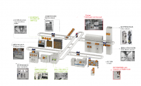
CD-SEM is an advanced fully automatic wafer online measurement equipment. It uses electron beam scanning imaging technology to monitor key process parameters during wafer manufacturing. It is used to measure the critical dimensions of photoresist after development and the contact hole diameter/through hole diameter and gate line width after etching. It is a key device to improve chip manufacturing yield and maintain product quality consistency. Huiran Microelectronics has mastered the underlying design capabilities and independently designed the electronic optical system, image processing algorithm, and high-speed wafer transmission system, providing important microscopic data for the multi-layer and complex integrated circuits.
Huiran Microelectronics stated that overcoming the "bottleneck project" requires unity of purpose. Huiran Microelectronics will work together with customers, suppliers, and partners to continue to overcome key technical difficulties such as electron beam stability and resolution, precise positioning and control, image enhancement and analysis, and improving measurement speed. It will accelerate product iteration, provide more high-performance and reliable options for the integrated circuit industry, and contribute its own strength to the industry.


