Chinese semiconductor thread II

tokenanalyst

Brigadier
Registered Member
BIT trying to solve the biggest issue with NIL overlay.​
NIL could really reduce the cost of manufacturing semiconductor devices, something that I think could be more important for the future than dimensional scaling.

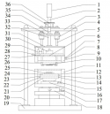
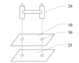
A multifunctional nanoimprint lithography device based on multi-layer alignment technology​

CN118131562A

Abstract​

The invention discloses a multifunctional nanoimprint lithography device based on multi-layer alignment technology, wherein a rotating workbench and a lower imprint cavity are installed on a base, and an X-Y axis moving workbench is installed inside the lower imprint cavity; the lower end of the bracket is fixed to the base, a planetary gear reducer is fixed to a support, the support is fixed to a crossbeam, and a coupling connects the output shaft of the planetary reducer to one end of a ball screw; the upper end of the guide rail is fixed to the crossbeam, and the inner hole of the linear bearing matches the outer diameter of the guide rail; a fixed plate is fixed to a support box, the support box is fixed to an upper imprint cavity, an electron microscope group and an ultraviolet light source are installed on an X-axis moving workbench, the X-axis moving workbench is fixed to the upper imprint cavity inside the support box, and a glass plate and a template fixture are installed in the upper imprint cavity. The invention can realize efficient and high-precision multi-layer nanostructure alignment imprinting, can perform two imprinting modes of ultraviolet imprinting and hot imprinting, and can also realize an imprinting process for complex curved surfaces.​

1718475503303.png1718475527786.png
 

henrik

Senior Member
Registered Member
This channel seems to have a lot of information about Chinese lithography machines development. Don't know if his information is legitimate at all.

ASML confirms that domestic lithography machines have reached what level? But ASML seems quite worried, is it afraid of losing the Chinese market?​


BlackWindMnt

Captain
Registered Member
Chinese wafer-scale designs. This seems somewhat important to my non-expert eye:

Please, Log in or Register to view URLs content!
Yeah its another way to increase computing powers. If you can't shrink the nano meter, you can always expand the area.
They are probably doing it on 22nm because of high yields. I do wonder how much bandwidth they can get with the network on chip and the more complex cache/memory hierarchy?
 

gelgoog

Lieutenant General
Registered Member
ASML wants to continue its leadership position by increasing the production rate of its lithography machine tools in addition to introducing Hyper-NA EUV.

But as someone from Intel once told me, the issue is the size of the lithography machine tool will continue to increase. You need to power the light source and drive the optics. The latest High-NA machine tool is already the size of a bus. Before the EUV machine tool was the size of a car. You need to design the fabs around the tools. Re-equipping old fabs with new tools becomes impossible.

Please, Log in or Register to view URLs content!

ASML Aims for Hyper-NA EUV, Shrinking Chip Limits​

06.12.2024

...
The company’s former president, Martin van den Brink, surprised experts with the announcement of the new “Hyper-NA” EUV technology that is still in the early stages of development, according to global R&D organization imec, which has worked closely with ASML. Hyper-NA would follow the High-NA systems that ASML installed early this year for the first time at an Intel semiconductor facility in the U.S. state of Oregon.

“Moving forward long term, we need to improve our illumination system, and we have to go to Hyper-NA,” van der Brink said in a May presentation at imec’s ITF World in Antwerp. “In parallel, we have to drive the productivity on all of our systems to 400 to 500 wafers per hour.”

Please, Log in or Register to view URLs content!
Productivity for DUV and EUV. (Source: ASML)

High-NA takes numerical aperture (NA) to 0.55 NA from the 0.33 NA of earlier EUV tools. About three years ago, the company said High-NA would help chipmakers reach process nodes well beyond 2 nm for at least 10 years. Now, ASML has said that around 2030, the company will offer Hyper-NA, reaching 0.75 NA, according to an image van den Brink showed at the imec event.
...
It was the first time that ASML added Hyper-NA EUV to their roadmap, according to Imec Advanced Patterning Program Director Kurt Ronse, who has developed lithography in cooperation with ASML for more than 30 years.

Please, Log in or Register to view URLs content!

ASML EUV roadmap. (Source: ASML)
“There’s a lot of research on going now,” he told EE Times. “Can we go higher than 0.55 to 0.75, 0.85? Hyper-NA certainly brings some new challenges.”

One of the problems is light polarization starting around 0.55 NA, according to Ronse.

“If you go higher than 0.55, very quickly you see that polarization is killing your contrast, because one of the polarization orientations is basically canceling out the light,” he said. “You would need polarizers in order to avoid that.” The downside is that polarizers block light, reduce power efficiency and increase production cost, he noted.

ASML is the world’s only company that makes the EUV tools that are indispensable for making chips with the highest transistor densities. Chip designers like Nvidia, Apple and AMD count on the EUV tools at leading foundry Taiwan Semiconductor Manufacturing Co. (TSMC) to make processors used in AI hardware and other high-performance computing equipment.

Two years ago, imec started working on Hyper-NA with computer simulations.

“Gradually you saw that more and more companies started to be interested in Hyper-NA and started their own studies,” Ronse said. “Zeiss were starting to make their lens designs, and gradually also ASML was becoming more open on Hyper-NA, but they never have put it on the roadmap before, as far as I know. It was always ending with 0.55 NA.”

Another challenge of Hyper-NA will be the resist.

“Already at 0.55 NA we will have thin down the resists,” Ronse said. “With Hyper-NA, it even gets worse. This will result in more challenges for etch selectivity”.

High-NA just starting

In April, Intel Foundry installed the industry’s first High-NA lithography system. Intel said the new tool provides the ability to dramatically improve resolution and feature scaling for the next generation of processors, enabling process leadership beyond Intel’s 18A process node that is roughly equivalent to TSMC’s upcoming 2-nm process. TSMC does not plan to install High-NA tools at this point.

“TSMC doesn’t need High-NA yet,” Ronse said. “Toward the end of this decade, they will likely introduce it.”

At present, TSMC can use its expertise in double-patterning together with its existing EUV tools, Ronse added.

“What is really critical in double patterning is the edge-placement error,” he said. “Your two masks have to be perfectly aligned. Intel wants to avoid that. The big difference with Intel is that they have not mastered double patterning as well as TSMC. As a result, they prefer a higher resolution with High-NA EUV.”

Other leading chipmakers that use EUV, such as Samsung, Micron and SK Hynix, are also considering High-NA.

High-NA should last through process nodes going from 2 nm to 14 angstroms, 10 angstroms and perhaps even 7 angstroms, according to Ronse. After that, Hyper-NA will start to take over, he added.

Hyper-NA will reduce the “dangerous trend” of double patterning, van den Brink said in his presentation.

“If you do double patterning, you have to do everything twice. That easily becomes more expensive,” Ronse said.

After High-NA

There are few alternatives to Hyper-NA once High-NA runs out of steam, Ronse says.

People have considered nanoimprint as a substitute, but the throughput is typically far below that of a High-NA scanner. There is also the idea of multi-beam electron-beam lithography, which eliminates the use of expensive photomasks by writing patterns directly to a silicon wafer. The only company that developed e-beam lithography tools, Netherlands-based Mapper, has gone out of business.

Outside of lithography, researchers have tried to shrink the size of transistors to continue scaling downward, but that approach is also reaching physical limits.

“You cannot imagine that there’s going to be devices of only 2 angstroms,” Ronse says. “It’s only two atoms. At some point, it has to stop.”

New materials will likely take the place of silicon, according to Ronse.

“There are new materials which have a higher mobility for electrons,” Ronse said. “These are much more difficult to put on the wafer. Research groups are working on that.”

The wafers will stay silicon, Ronse notes.

“It’s only for a few levels that you will have to deposit a very thin layer where the electrons have to go through. What will be needed is dedicated equipment that can uniformly deposit that over a whole wafer. Right now, it’s in the labs. It’s only on small areas one is working on. There will be new deposition tools. Also, etching these materials may be more difficult, so we need new etching techniques. The basis of the chip will still be silicon.”
 

LuzinskiJ

Junior Member
Registered Member
Yeah its another way to increase computing powers. If you can't shrink the nano meter, you can always expand the area.
They are probably doing it on 22nm because of high yields. I do wonder how much bandwidth they can get with the network on chip and the more complex cache/memory hierarchy?
This transfer of complexity is typical in engineering, if you can't solve something in one area, than transform that something into something else maybe equally complex in other areas which you have a chance of solving as long as the requirements are flexible enough for you to do so. These guys must think they can do a equivalent job of coding up a network switch and distributed cache to produce a Thévenin-equivalent
 

ansy1968

Brigadier
Registered Member
ASML wants to continue its leadership position by increasing the production rate of its lithography machine tools in addition to introducing Hyper-NA EUV.

But as someone from Intel once told me, the issue is the size of the lithography machine tool will continue to increase. You need to power the light source and drive the optics. The latest High-NA machine tool is already the size of a bus. Before the EUV machine tool was the size of a car. You need to design the fabs around the tools. Re-equipping old fabs with new tools becomes impossible.

Please, Log in or Register to view URLs content!

ASML Aims for Hyper-NA EUV, Shrinking Chip Limits​

06.12.2024

...
The company’s former president, Martin van den Brink, surprised experts with the announcement of the new “Hyper-NA” EUV technology that is still in the early stages of development, according to global R&D organization imec, which has worked closely with ASML. Hyper-NA would follow the High-NA systems that ASML installed early this year for the first time at an Intel semiconductor facility in the U.S. state of Oregon.

“Moving forward long term, we need to improve our illumination system, and we have to go to Hyper-NA,” van der Brink said in a May presentation at imec’s ITF World in Antwerp. “In parallel, we have to drive the productivity on all of our systems to 400 to 500 wafers per hour.”

Please, Log in or Register to view URLs content!
Productivity for DUV and EUV. (Source: ASML)

High-NA takes numerical aperture (NA) to 0.55 NA from the 0.33 NA of earlier EUV tools. About three years ago, the company said High-NA would help chipmakers reach process nodes well beyond 2 nm for at least 10 years. Now, ASML has said that around 2030, the company will offer Hyper-NA, reaching 0.75 NA, according to an image van den Brink showed at the imec event.
...
It was the first time that ASML added Hyper-NA EUV to their roadmap, according to Imec Advanced Patterning Program Director Kurt Ronse, who has developed lithography in cooperation with ASML for more than 30 years.

Please, Log in or Register to view URLs content!

ASML EUV roadmap. (Source: ASML)
“There’s a lot of research on going now,” he told EE Times. “Can we go higher than 0.55 to 0.75, 0.85? Hyper-NA certainly brings some new challenges.”

One of the problems is light polarization starting around 0.55 NA, according to Ronse.

“If you go higher than 0.55, very quickly you see that polarization is killing your contrast, because one of the polarization orientations is basically canceling out the light,” he said. “You would need polarizers in order to avoid that.” The downside is that polarizers block light, reduce power efficiency and increase production cost, he noted.

ASML is the world’s only company that makes the EUV tools that are indispensable for making chips with the highest transistor densities. Chip designers like Nvidia, Apple and AMD count on the EUV tools at leading foundry Taiwan Semiconductor Manufacturing Co. (TSMC) to make processors used in AI hardware and other high-performance computing equipment.

Two years ago, imec started working on Hyper-NA with computer simulations.

“Gradually you saw that more and more companies started to be interested in Hyper-NA and started their own studies,” Ronse said. “Zeiss were starting to make their lens designs, and gradually also ASML was becoming more open on Hyper-NA, but they never have put it on the roadmap before, as far as I know. It was always ending with 0.55 NA.”

Another challenge of Hyper-NA will be the resist.

“Already at 0.55 NA we will have thin down the resists,” Ronse said. “With Hyper-NA, it even gets worse. This will result in more challenges for etch selectivity”.

High-NA just starting

In April, Intel Foundry installed the industry’s first High-NA lithography system. Intel said the new tool provides the ability to dramatically improve resolution and feature scaling for the next generation of processors, enabling process leadership beyond Intel’s 18A process node that is roughly equivalent to TSMC’s upcoming 2-nm process. TSMC does not plan to install High-NA tools at this point.

“TSMC doesn’t need High-NA yet,” Ronse said. “Toward the end of this decade, they will likely introduce it.”

At present, TSMC can use its expertise in double-patterning together with its existing EUV tools, Ronse added.

“What is really critical in double patterning is the edge-placement error,” he said. “Your two masks have to be perfectly aligned. Intel wants to avoid that. The big difference with Intel is that they have not mastered double patterning as well as TSMC. As a result, they prefer a higher resolution with High-NA EUV.”

Other leading chipmakers that use EUV, such as Samsung, Micron and SK Hynix, are also considering High-NA.

High-NA should last through process nodes going from 2 nm to 14 angstroms, 10 angstroms and perhaps even 7 angstroms, according to Ronse. After that, Hyper-NA will start to take over, he added.

Hyper-NA will reduce the “dangerous trend” of double patterning, van den Brink said in his presentation.

“If you do double patterning, you have to do everything twice. That easily becomes more expensive,” Ronse said.

After High-NA

There are few alternatives to Hyper-NA once High-NA runs out of steam, Ronse says.

People have considered nanoimprint as a substitute, but the throughput is typically far below that of a High-NA scanner. There is also the idea of multi-beam electron-beam lithography, which eliminates the use of expensive photomasks by writing patterns directly to a silicon wafer. The only company that developed e-beam lithography tools, Netherlands-based Mapper, has gone out of business.

Outside of lithography, researchers have tried to shrink the size of transistors to continue scaling downward, but that approach is also reaching physical limits.

“You cannot imagine that there’s going to be devices of only 2 angstroms,” Ronse says. “It’s only two atoms. At some point, it has to stop.”

New materials will likely take the place of silicon, according to Ronse.

“There are new materials which have a higher mobility for electrons,” Ronse said. “These are much more difficult to put on the wafer. Research groups are working on that.”

The wafers will stay silicon, Ronse notes.

“It’s only for a few levels that you will have to deposit a very thin layer where the electrons have to go through. What will be needed is dedicated equipment that can uniformly deposit that over a whole wafer. Right now, it’s in the labs. It’s only on small areas one is working on. There will be new deposition tools. Also, etching these materials may be more difficult, so we need new etching techniques. The basis of the chip will still be silicon.”
Then SSMB seems more economical and commercially viable compare to both HI NA and HYPER NA.
 

Hyper

Junior Member
Registered Member
Then SSMB seems more economical and commercially viable compare to both HI NA and HYPER NA.
No. It isn't. They are two different things. One refers to the light source and other refers to the optics. You seem to have blind faith in synchrotron light sources.
 

Wrought

Junior Member
Registered Member
Seems like new materials like graphene or whatever are a perfect opportunity to reset the board, as it were, for semiconductor technology. Just like ICE->NEV, the switch over to a new solution for the same problem opens opportunities for historical laggards to catch up or even outpace historical leaders. Of course, it's much easier to say in hindsight.
 
Top