You are using an out of date browser. It may not display this or other websites correctly.
You should upgrade or use an alternative browser.
You should upgrade or use an alternative browser.
Chinese semiconductor thread II
- Thread starter vincent
- Start date
Hi bro my assumption is that SN1 produced its first 14nm in 2019.
Truth to be told, SMIC has been producing chips using its 14nm-class manufacturing technology since late 2019 (one of the products is Huawei's HiSilicon Kirin 710A) at its SN1
N+1 is a sub 10nm is a experimental chip equivalent to Samsung 8nm, as they transition their production line for N+2 7nm line. Here I think a domestic solution may have found for 14nm line, Tianjin and Shenzhen FAB (the Chinese refer them as 28nm FAB line) come to mind.
As @tphuang mentioned SN1 had a capacity of 35k WPM in 2023 and SN2 after finishing its construction is still calibrating its ASML equipment and may have start operation in 2024. And all Shanghai FAB will be using ASML machine even the rumored Huawei FAB (obtain 2 2nd hand NXT 1980i) as they had an established eco system.
SO where did China gets its 14nm chip? Nobody seems to talk about it anymore like yesterday news. And what about the recently finished SMIC Beijing FAB? IF we connect the dot maybe SMIC Beijing is the new 7nm domestic line that the article may have assume. Bro,
Bro
12nm or 12nm/14nm is not a thing of the past.
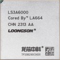
Assuming Loongson latest 3A6000 is manufactured by SMIC currently.
Is that means SN1 is being divided to multiple lines?. One for Loongson's 12nm, One for Huawei's 7nm and what else are there in SN1?
its said Huawei used SMIC and JHCC for foundry services. Wonder what JHCC is producing?
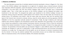
Domestic SM Equipment is already being use by Shanghai ICRD in the development of China GAAFET lines.
The domestic Si/SiGe CVD tool is already being tested and Naura ICP etching tools already being used that means that AMEC etching tools are also good enough for GAAFET lines.
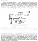
MultiChamber CVD-ALD tool develop but CAS and Shanghai ICRD.
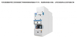
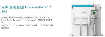
Some Metrology tools
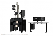
TEM
The domestic Si/SiGe CVD tool is already being tested and Naura ICP etching tools already being used that means that AMEC etching tools are also good enough for GAAFET lines.

MultiChamber CVD-ALD tool develop but CAS and Shanghai ICRD.


Some Metrology tools

TEM

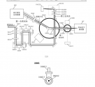
Ultra-high space-time resolution pumping detection system based on high-order harmonic extreme ultraviolet light source.
CN118130414A
Peking University
Abstract
The application discloses an ultra-high space-time resolution pumping detection system based on a high-order harmonic extreme ultraviolet light source, and belongs to the field of ultra-fast optics. In the system, a pulse laser outputs fundamental frequency light, and a continuous laser outputs continuous laser. The dichroic mirror performs beam combination processing on the fundamental frequency light and the continuous laser light to obtain mixed light. The beam splitter splits the mixed light into driving light and detection light, the driving light propagates to the higher harmonic generation device along a first direction, and the detection light propagates to the focusing beam combining device along a second direction. The harmonic generation device generates a harmonic beam using the driving light. The focusing beam combining device filters the high-order harmonic beam to obtain extreme ultraviolet light, and combines the extreme ultraviolet light with the detection beam to obtain first combined beam. The charged particle detector detects charged particles generated by interaction of the first combined beam with the target gas target in a pump detection experiment. The application realizes a pumping detection system with ultra-high resolution in two dimensions of time and momentum space.
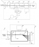
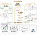
Neural network driven sensitivity analysis of diffraction-based overlay metrology performance to target defect features
Electrical Engineering, Nanjing University of Aeronautics and Astronautics
National Key Laboratory of Microwave Photonics
Key Laboratory of Aerospace Integrated Circuits and Microsystem, Ministry of Industry and Information Technology
State Key Laboratory of Precision Measurement Technology and Instruments, Department of Precision Instrument,
Tsinghua University
National Key Laboratory of Microwave Photonics
Key Laboratory of Aerospace Integrated Circuits and Microsystem, Ministry of Industry and Information Technology
State Key Laboratory of Precision Measurement Technology and Instruments, Department of Precision Instrument,
Tsinghua University
Abstract
Overlay (OVL) is one significant performance indicator for the lithography process control in semiconductor manufacturing. The accuracy of the OVL metrology is extremely critical for guarantee the lithography quality. Currently, diffraction-based overlay (DBO) is one of the mainstream OVL metrology techniques. Unfortunately, the accuracy of the DBO metrology is largely affected by the defect features of the OVL target. Therefore, there is a strong need to investigate the impacts of these target defects on the DBO metrology performance. However, efficiently investigating the statistical and interactive impacts of various DBO target defects remains challenging. This study aims to address this issue through proposing an intelligent sensitivity analysis approach. A cumulative distribution based global sensitivity analysis (GSA) method is utilized to assess the nonlinear influences of multiple defects in the OVL target on the DBO inaccuracy. The scenarios with both known and unknown distributions of the OVL target defects are considered. For the former, a neural network driven forward model is constructed for fast calculating the optical diffraction responses to accelerate the GSA process. For the latter, another neural network based inverse model are built for efficiently estimating the distribution of the target defects. Finally, a series of simulation experiments are conduct for typical DBO targets with multiple common defect features. The results demonstrate the effectiveness and robustness of the proposed approach as well as give valuable insights into the DBO defect analysis. Our study provides a strong tool to assist the practitioners in achieving intelligent and efficient DBO analysis and thus in enhancing OVL metrology performance.

KAISHITONG RECEIVED MULTIPLE REPEAT ORDERS FROM KEY WAFER FAB CUSTOMERS
Recently, Shanghai Kaishitong Semiconductor Co., Ltd. has once again received a repeat order for a low-energy, large-beam ion implanter from a 12-inch mainstream wafer fab customer. This key customer has purchased equipment from Kaishitong many times since the first quarter of last year, with a total order of more than 10 units.
Since 2024, Kaishitong's ion implanter has continued to serve the industrialized mass production of customers in many locations, and the number of shipments has exceeded 10 in less than half a year. As Kaishitong's flagship product, the low-energy, large-beam ion implanter condenses years of engineering experience and has been verified by large-scale production lines. It has high beam transmission efficiency and good stability, and has excellent process matching capabilities and a wide range of process coverage capabilities, which are widely favored by customers.
In the future, Kaishitong will continue to adhere to the customer-centric development concept, continue to innovate and continuously improve, provide customers with more outstanding equipment and service solutions, help customers reduce costs and increase efficiency, and work with customers to promote the prosperity and progress of the integrated circuit industry.
I think an interesting thing that was pointed out on semiwiki is that Huawei/SMIC could go straight into GAAFET using just a minor modification of the Finfet process.Domestic SM Equipment is already being use by Shanghai ICRD in the development of China GAAFET lines.
The domestic Si/SiGe CVD tool is already being tested and Naura ICP etching tools already being used that means that AMEC etching tools are also good enough for GAAFET lines.
View attachment 131069
MultiChamber CVD-ALD tool develop but CAS and Shanghai ICRD.
View attachment 131074
View attachment 131073
Some Metrology tools
View attachment 131071
TEM
View attachment 131075
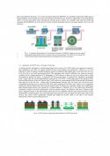
SinoCera Materials: SinoCeramic Saichuang Precision Products Project Starts Construction.
Recently, Sinocera Materials' wholly-owned subsidiary, Sinocera Saichuang Electric (Tongling) Co., Ltd., held a groundbreaking ceremony for a ceramic metallization project in the Tongling Economic Development Zone, Anhui Province. The project has a total investment of 150 million yuan and will build a 2# plant, a comprehensive building B, and a 2# auxiliary building project with a total area of 28,000 square meters, creating a high-end ceramic metallization product production line dominated by the company's own core technology.
After the project expansion, the various ceramic thin film metallization products undertaken by Sinoceramics Saichuang will guide the company to enter the application fields of thin sensors, microwave radar devices, laser heat sinks, power supply modules, IGBT and other high-end precision ceramic products. This project can improve the production efficiency and product delivery capabilities of existing products, promote the company's technological innovation and manufacturing capabilities to a new level, and will break the dilemma of high-end ceramic metallization products being monopolized by foreign technology.
In addition, Sinoceramic Materials' ceramic balls are considered the main solution to the electrical corrosion problem of new energy vehicles. Compared with steel balls, they are more suitable for high-speed motor usage scenarios. With the rapid development of the global new energy industry, the demand for ceramic balls will continue to increase. The company is proficient in the key technologies from powder preparation to ceramic ball manufacturing. The silicon nitride ceramic bearing ball products of its subsidiary Sinoceramic Jinsheng have been successfully verified by many mainstream bearing manufacturers, and their performance has reached the international advanced level.


