Semiconductor device and manufacturing method thereof
IMECASCN117913122A
Abstract
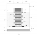
The application provides a semiconductor device and a method for manufacturing the same, the semiconductor device includes: the source electrode, the drain electrode, the grid electrode and the channel structure are arranged on one side of the substrate, the channel structure comprises a lamination formed by a plurality of nano sheets, and the grid electrode surrounds the nano sheets. In the present application, the substrate may include a first substrate and a second substrate which are sequentially stacked, wherein the first substrate is a semiconductor material and the second substrate is an insulating material, that is, the substrate of the present application is a semiconductor-on-insulator substrate, so that the performance of GAAFET can be optimized. The semiconductor device provided by the application comprises the isolation structure, wherein the isolation structure is arranged between the channel structure and the second substrate, and extends to the source electrode and the drain electrode in the direction parallel to the plane of the substrate, so that effective isolation is formed among the substrate, the grid electrode, the drain electrode and the source electrode, and parasitic channel leakage of the substrate is restrained by utilizing the isolation structure, thereby reducing off-state leakage current of the device under the condition of shorter grid length and improving the integral performance of the device.

