Chinese semiconductor thread II

tokenanalyst

Brigadier
Registered Member

Baoying Gas Nanjing Ultra-High Purity Ammonia (Photoelectronic Grade) Production Center Project Started​


Recently, the Nanjing Special Gas Production Center project invested by Baoying (Nanjing) Gas Co., Ltd. started construction.
The Nanjing Special Gas Production Center project plans to use a combination of adsorption, distillation and ultrafiltration purification technology to build Nanjing's first 8,000 tons/year ultra-high purity ammonia (photoelectronic grade) production center. After completion, the production center will help improve the advanced new material industry chain in the integrated circuit field of Jiangbei New District and enhance the overall scientific and technological level and competitiveness of the integrated circuit industry in Nanjing and Jiangbei New District.

It is reported that ultra-high purity ammonia (photoelectronic grade) has a wide range of applications in the field of optoelectronics. It is an important raw material in optoelectronics and microelectronics such as semiconductor lighting, integrated circuits, flat panel display panels, and solar cells. Its quality directly affects the optical and electrical properties of the material and even the service life of the equipment. Ultra-high purity ammonia (photoelectronic grade) is used in the manufacture of semiconductor lighting devices such as LEDs and lasers, silicon wafers and metal wires in integrated circuits, and flat panel display panels such as liquid crystal displays and organic light-emitting diodes.

Official news from Nanjing Jiangbei New District showed that the New Materials Science and Technology Park and Baoying (Nanjing) Gas Co., Ltd. also signed a contract for the East China Gas (Hydrogen Energy) Storage and Transportation Center Project. The East China Gas (Hydrogen Energy) Storage and Transportation Center Project aims to build its own Class II hazardous chemical logistics and transportation fleet and product distribution information system to achieve product safety, intelligent logistics and cost control under different filling methods and multiple parameters. At the same time, through data empowerment and independent research and development, it will establish a gas e-commerce trading platform open to upstream and downstream, improve supply chain system management and intelligent data analysis, and enhance the core competitiveness of enterprises.

On December 29, 2023, Baoying (Nanjing) Gas Co., Ltd. announced the completion of a total of 400 million yuan in financing for Round B and Round B+. The investors include Cathay Capital, Bocom Capital, Hengxu Capital, and Xiamen International Trade Fund Investment.

Please, Log in or Register to view URLs content!
 

tokenanalyst

Brigadier
Registered Member
XMC initiates IPO in Chinese competitive foundry market

NOR Flash manufacturer Wuhan Xinxin Semiconductor Manufacturing Co. (XMC) recently disclosed an IPO counseling filing with the Hubei Securities Regulatory Bureau, according to the official website of the China Securities Regulatory Commission. Its recently announced bidding project may indicate its ambition to become China’s first HBM foundry, according to the report by Chinese media Semi Insights.

As per information from its website, XMC provides 12-inch foundry services for NOR Flash, CIS, and Logic applications with processes of 40 nanometers and above. Originally a wholly-owned subsidiary of Yangtze Memory Technologies (YMTC), XMC announced in March its first external financing round, increasing its registered capital from approximately CNY 5.782 billion to about CNY 8.479 billion. Its IPO counseling filing also indicates that it is still majority-owned by YMTC, with a shareholding ratio of 68.1937%.

XMC builds a full-loop & one-stop CIS (CMOS Image Sensor) technology platform. XMC has mass production capability of high-performance, low-power image sensor products. This technology can be widely used in smartphones, automotive electronics, machine vision, professional imaging and other market segments.

Please, Log in or Register to view URLs content!
 

tokenanalyst

Brigadier
Registered Member

High-end polishing solution provider "Puresun" completed tens of millions of yuan in Pre-A round of financing.​

Wuxi Puruisheng New Materials Technology Co., Ltd. (hereinafter referred to as "Puresheng New Materials" or "the Company") completed a Pre-A round of financing of 10 million yuan. In this investment, the company's old shareholders, Nuoyan Capital, Zhongnan Venture Capital Fund, and Wuxi Yunlin Fund continued to increase their holdings. At present, the company's high-end alumina polishing abrasives and polishing liquids are ready for mass production. The funds raised in this round will further consolidate the company's operational capabilities and ensure that the company can quickly expand production after being verified by downstream customers.

Founded in April 2023, Presun New Materials is committed to becoming a first-class domestic supplier of high-end polishing solutions. The company has profound technical accumulation in the field of high-end abrasives, focusing on the research and development of high-end alumina polishing liquid, alumina polishing abrasives and other products. The products can be used for the polishing of integrated circuits, compound substrates, paint surfaces, optical lenses, metals and other materials.

Please, Log in or Register to view URLs content!
 

tphuang

Lieutenant General
Staff member
Super Moderator
VIP Professional
Registered Member
The Indian origin woman behind the US tech sanctions:

Please, Log in or Register to view URLs content!

Key quote:

“When I do travel — and by overseas l mean Taiwan, Japan, Korea, Switzerland, Germany, the Netherlands, U.K., you know, allied countries — almost to a person, they don’t really understand what the national security objective is that the U.S. government is trying to accomplish with all these new controls,” said Wolf, the former assistant commerce secretary.

Some, such as Atkinson, say the grants for building new U.S. technological hubs have been distributed too diffusely.

“The whole point of this was you can’t have 50 places,” he said. “There’s not enough money. There’s not enough technology to go around.”


Another interesting article:

Please, Log in or Register to view URLs content!

Key paragraph:

Will a successful implementation of the four above measures remove the threat of China’s control over certain global supply chains? No. It will only buy time for the West. If everything goes well with implementation, it will increase the production capacity of the Western economies in the chips sector. But then to whom will these newly added mature chips be sold given that these economies are overwhelmingly de-industrialized? Perhaps again to China, where local industry still grows steadily. Currently, this is the case with the US corporation Applied Materials, which makes about 45% of its revenue from China and will probably lose it like other similar big producers in the West if the latter invests more into mature chips.
I don't know what is up with the need to point out someone's ethnicity in these discussions, since the decision was made across the entire US political class. But it did not nothing except taking this thread off topic.

So please be mindful of this with your posting going forward
 

tokenanalyst

Brigadier
Registered Member
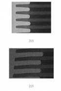
Direct Writing Lithography is a must for mask and mold manufacturing for projection and imprint lithography, this work looks to increase the productivity of these machines.

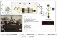
Fiber-optic multi-channel parallel laser direct writing lithography system​

Abstract

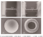
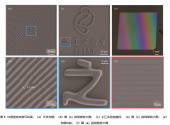
Direct laser writing (DLW) has the advantages of writing any three-dimensional structure without mask plates, in a simple process flow, and with minimal environmental requirements, and it finds widespread application in micro/nano processing technology. However, owing to throughput limits, single-channel DLW cannot be used for large-area fabrication. Currently, instead of single-channel, multi-channel parallel writing is the most direct and effective approach. The reported methods for generating multiple beams typically rely on the construction of a spatial light path, which has been extensively studied. However, challenges persist in generating large numbers of channels. Issues such as poor spot uniformity, independent modulation problems, and system complexity hinder further application of the DLW technology. To improve the throughput of the DLW technology, we designed and verified a multi-channel parallel lithography technology. This technology can achieve a manufacturing accuracy of 126 nm transversely and 222 nm longitudinally under the condition of a picosecond pulse width, and it can process large-area complex patterns and three-dimensional structures.

1717450916045.png
1717450987601.png1717451017730.png

Please, Log in or Register to view URLs content!


gotodistance

New Member
Registered Member
On May 30, Huawei Managing Director and Huawei Cloud CEO Zhang Ping'an attended the China Mobile Computing Conference and told industry colleagues: "We definitely can't get 3nm, we can't get 5nm, “It would be great if we could solve 7 nanometers,” he admitted. ”

Zhang Ping'an said that due to the dilemma of the chip manufacturing process, the direction of innovation can no longer rely on single-point chip processing, but can only rely on system architecture innovation. For domestic chip manufacturers, it will be difficult to produce chips below 7nm for a long time to come.

Has Huawei failed to mass produce 5 nanometers?

Please, Log in or Register to view URLs content!
 

tokenanalyst

Brigadier
Registered Member
On May 30, Huawei Managing Director and Huawei Cloud CEO Zhang Ping'an attended the China Mobile Computing Conference and told industry colleagues: "We definitely can't get 3nm, we can't get 5nm, “It would be great if we could solve 7 nanometers,” he admitted. ”

Zhang Ping'an said that due to the dilemma of the chip manufacturing process, the direction of innovation can no longer rely on single-point chip processing, but can only rely on system architecture innovation. For domestic chip manufacturers, it will be difficult to produce chips below 7nm for a long time to come.

Has Huawei failed to mass produce 5 nanometers?

Please, Log in or Register to view URLs content!
I think that was a quote from a Taiwanese publication. I don't know what it is, but lately they have this nasty habit of putting words in other people mouths, like if they are desperate for something.

The reality is that nobody knows, China semiconductor industry is a black box now. I don't think there is nothing stopping Huawei and SMIC from reaching 5nm, if TSMC didn't have EUV they will still making chips using DUVi, using SAQP or another patterning techniques. Back at 2022 everybody including a lot of experts inside China where hell bent that was impossible for SMIC and Huawei to make 7nm chips in volume, they demonstrated the contrary, a win for multiple patterning techniques. I myself was expecting that it would take them a lot longer to reach 7nm in volume and they surprise me.
 

tokenanalyst

Brigadier
Registered Member
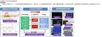
NAURA GAAFET Etching Machine

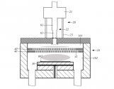
Method for forming semiconductor structure, plasma generating device and semiconductor process equipment​

CN117650047 A​

Abstract​

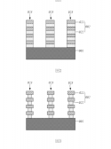
The invention discloses a method for forming a semiconductor structure, a plasma generating device and semiconductor process equipment, which belong to the technical field of semiconductors, and the disclosed method comprises the following steps: performing a first etching process on the semiconductor laminated structure to form a plurality of fin-shaped structures which are spaced from each other; the semiconductor laminated structure comprises at least one first semiconductor layer and at least one second semiconductor layer which are alternately stacked, wherein a first interval is formed between a plasma generating cavity and a reaction cavity when a first etching process is performed; a second etching process is performed on the fin structure to selectively etch at least a portion of one of the first semiconductor layer and the second semiconductor layer, the second etching process being performed to space the plasma generation cavity from the reaction chamber by a second spacing, the second spacing being greater than the first spacing. The scheme can solve the problem that the etching yield is low due to the fact that the cavity needs to be replaced in the process of carrying out different types of etching processes of semiconductor process equipment.​

1717456370386.png1717456407353.png
1717456426595.png
 
Top