Chinese semiconductor thread II

tokenanalyst

Brigadier
Registered Member
Looks like there is another group of companies that are slowly crawling up creating a sort of secondary supply chain for semiconductor optical lithography apart from the establish companies of the project 02.

I have seen new companies in:

- High end wafer precision motion.
- High end lithography optics.
- High end positioning sensing.
- High end excimer light sources.
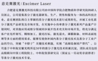

1717192767936.png

This companies for now are serving other sectors like metrology equipment and so on but there is a possibility that we are going to see DUV scanners from other company apart from SMEE and ASML and others in China.

In that case my guess is that ASML and Nikon may use their patent portfolio to try to stop any company in China apart from SMEE from developing DUV lithography machines so they don't have so many competitors cabbagetizating the lithography industry.
 

tphuang

Lieutenant General
Staff member
Super Moderator
VIP Professional
Registered Member
More intersection of radar industry and semi here

Please, Log in or Register to view URLs content!

this lady is award price for
中国电科14所微电路总装师顾春燕,长期致力于百余型重点装备的探索、研发与制造,实现国内首个10微米金丝键合TR组件的工程化研制和生产,其精湛的技艺助力陆、海、空、天等各型雷达装备核心组件全流程技术攻关。曾荣获“江苏省技术能手”、“江苏省五一劳动奖章”、“江苏好人”,中国电科“最美电科人”等荣誉。
engineering development and production of the first 10-micron gold wire bonding TR component in China. says she is involved in land, sea, air & space type of radar

just looking at this page here
Please, Log in or Register to view URLs content!
it mentions 18 to 50 micron diameter gold wire bonding.

This one here says they can do up to 15 micron for very fine application
Please, Log in or Register to view URLs content!

So 10 micron is pretty world class.

It seems to me that thinner gold wire bonding would be important here in miniaturization.
as for why gold
ur 2N gold bonding wires have been specifically designed to withstand the harsh temperature cycles and high temperature storage conditions.
Seems like it's ability to withstand harsh temperature, which is needed for weapon system
 
Last edited:

measuredingabens

Junior Member
Registered Member
Please, Log in or Register to view URLs content!

Reliable wafer-scale integration of two-dimensional materials and metal electrodes with van der Waals contacts​

Abstract​

Since the first report on single-layer MoS2 based transistor, rapid progress has been achieved in two-dimensional (2D) material-based atomically thin electronics, providing an alternative approach to solve the bottleneck in silicon device miniaturization. In this scenario, reliable contact between the metal electrodes and the subnanometer-thick 2D materials becomes crucial in determining the device performance. Here, utilizing the quasi-van der Waals (vdW) epitaxy of metals on fluorophlogopite mica, we demonstrate an all-stacking method for the fabrication of 2D devices with high-quality vdW contacts by mechanically transferring pre-deposited metal electrodes. This technique is applicable for complex device integration with sizes up to the wafer scale and is also capable of tuning the electric characteristics of the interfacial junctions by transferring selective metals. Our results provide an efficient, scalable, and low-cost technique for 2D electronics, allowing high-density device integration as well as a handy tool for fundamental research in vdW materials.
 

olalavn

Senior Member
Registered Member
Looks like there is another group of companies that are slowly crawling up creating a sort of secondary supply chain for semiconductor optical lithography apart from the establish companies of the project 02.

I have seen new companies in:

- High end wafer precision motion.
- High end lithography optics.
- High end positioning sensing.
- High end excimer light sources.


View attachment 130410

This companies for now are serving other sectors like metrology equipment and so on but there is a possibility that we are going to see DUV scanners from other company apart from SMEE and ASML and others in China.

In that case my guess is that ASML and Nikon may use their patent portfolio to try to stop any company in China apart from SMEE from developing DUV lithography machines so they don't have so many competitors cabbagetizating the lithography industry.
No one knows the progress of domestic photolithography machines. Huazhuo Precision Technology has updated its listing materials, and the R&D costs of the immersion worktable have dropped a lot. However, the related parts projects have been developed. we guess the technical research and development of the immersion worktable is almost coming to an end. As for when it can be put into production, it isn't known yet.
 

tokenanalyst

Brigadier
Registered Member
No one knows the progress of domestic photolithography machines. Huazhuo Precision Technology has updated its listing materials, and the R&D costs of the immersion worktable have dropped a lot. However, the related parts projects have been developed. we guess the technical research and development of the immersion worktable is almost coming to an end. As for when it can be put into production, it isn't known yet.
I was not referring to U-precision, RSLASER, SMEE and the other companies involved in lithography in China, I was referring to a secondary supply chain that could allow smaller lithography startups to enter the projection lithography market.

Lithography is the most monopolized segment in the semiconductor industry, companies like ASML and Nikon either have exclusive suppliers that only sell to them or they manufacture everything in-house, SMEE is a monopoly on its own. But if more startups can enter the lithography equipment market the costs for lithography could be reduced considerably and you could see more innovations. That could only happen if there is more independent lithography sub-systems and part suppliers.
 

tokenanalyst

Brigadier
Registered Member

Focuslight Technology invests 500 million to build a new pan-semiconductor process photonic application solution industrial base project​


Recently, the pan-semiconductor process photonic application solution industrial base project invested by Xi'an Focus Technology Co., Ltd. (hereinafter referred to as " Focus Technology") in Hefei High-tech Zone obtained the "Construction Project Construction Permit" and started construction on site simultaneously.

It is understood that the project is located at the northeast corner of the intersection of Innovation Avenue and Baiyanwan Road in Hefei High-tech Zone, covering an area of about 39.8 acres. The planned investment is 500 million yuan to build three production plants and supporting facilities with a total construction area of about 79,000 square meters.

Juguan Technology said that it will leverage its accumulated technical advantages and rich product development experience in the field of pan-semiconductor applications to deploy the company's existing pan-semiconductor businesses such as solid laser lift-off LLO, Mini/Micro LED laser line spot Reflow, and semiconductor integrated circuit wafer annealing in Hefei, as well as new businesses under development such as solar cell applications, flat panel display solid laser annealing SLA, and semiconductor integrated circuit processes.

According to public information, Juguan Technology was established in 2007 and is mainly engaged in the research, development, production and sales of high-power semiconductor laser components and raw materials, and laser optical components in the upstream of the photonics industry. It focuses on the three major application directions of automotive applications, pan-semiconductor processes, and medical health, and provides upstream core components and midstream photonics application solutions to different customers.

Among them, in the field of pan-semiconductor processes, Focuslight Technology has laid out three major areas: chip process, chip advanced packaging laser-assisted bonding, and new display. In the field of new display, it has completed the product iteration development of the Mini LED Repair laser system, and at the same time, it is promoting the design of Micro LED mass transfer laser systems for customer needs and has entered the product development stage.

Please, Log in or Register to view URLs content!
 

tokenanalyst

Brigadier
Registered Member

Assistant Researcher Si Jia from the Carbon-Based Electronics Research Center has developed a new Ising computer​


Traditional general-purpose computing can no longer meet the ever-increasing demand for information processing. Future computing models are booming in the direction of being more specialized and more energy-efficient. Ising computing is a new computing technology that is used to solve complex problems that cannot be solved in polynomial time (Non-deterministic polynomial-time (NP)-hard problems), such as combinatorial optimization, large number decomposition, image processing, key cracking, and other fields. Current Ising computers are mostly built based on technologies such as optical fiber, memristor, nano oscillator, and complementary metal oxide semiconductor (CMOS). They have problems such as hardware redundancy, limited scale, and high energy consumption.

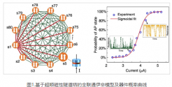
Assistant researcher Si Jia from the School of Electronics and the Center for Carbon-based Electronics Research at Peking University proposed a solution to use a special spin device, a superparamagnetic tunnel junction, to construct an Ising spin unit and then build an Ising computer. The device has a low energy barrier (<15K BT ) and can present a high-resistance or low-resistance state with a certain probability over time when disturbed by thermal noise at room temperature. The probability is determined by the current flowing through the device and can be fitted with a sigmoidal curve, as shown in Figure 1. This characteristic curve is highly consistent with the Boltzmann distribution probability curve of the Ising spin unit, and can be implemented in hardware simply and efficiently.
1717256109236.png
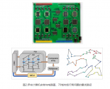
In the experiment, 80 superparamagnetic tunnel junctions were integrated on a PCB board, and a fully functional 80-node Ising computer was realized through peripheral circuit control. The traveling salesman problem of 70 cities was successfully solved through algorithm design (this problem usually requires 4761 nodes), as shown in Figure 2. Compared with the existing Ising computers, this work has the highest energy efficiency.

1717256153518.png
Please, Log in or Register to view URLs content!
 

tokenanalyst

Brigadier
Registered Member
PKU and Faraday lasers for high end sensing applications including high end interferometers and gratings sensors.​

PKU School of Electronics and Faraday Laser won the first prize of the China Institute of Metrology and Testing Science and Technology Progress Award​


Recently, the China Society for Metrology and Testing announced the list of winners of the 2023 China Society for Metrology and Testing Science and Technology Progress Award. The "Self-locked Atom-stabilized Semiconductor Laser System and Application" project led by Professor Chen Jingbiao of the School of Electronics won the first prize .

Award-winning achievement: Self-locked atom-stabilized semiconductor laser system and its application

Atomic frequency-stabilized semiconductor laser systems are basic instruments for conducting cutting-edge science in the field of quantum precision metrology. They are widely used in quantum precision metrology, atomic physics, atomic clocks, atomic gravimeters, and atomic gyroscopes. They are of strategic significance to national basic scientific research, economic development, and security construction. However, my country's current research on frequency-stabilized semiconductor laser systems is relatively weak, with more than 95% of its products relying on imports, resulting in a serious "bottleneck" problem. In addition, the frequency-stabilized semiconductor laser systems sold on the market have limitations such as insufficient stability, complex operation, and bulky size, which severely limit their application scenarios and scope.

In response to the demand for self-locking high-frequency-stable lasers in the fields of quantum precision metrology, atomic physics, and national defense equipment, the project team has made breakthroughs in key technologies such as high signal-to-noise ratio speed grating spectroscopy and modulation transfer spectrum feature identification self-locking, and successfully developed a self-locking atomic frequency-stabilized semiconductor laser system, and achieved industrial promotion and application in atomic clocks, gravimeters, interferometers and other equipment in the field of quantum precision metrology. New sales of 21.2344 million yuan and new profits of 2.704 million yuan. 41 papers were published, cited 234 times, and 25 patents were applied for and authorized.

Academician Li and other experts commented: "The overall technical achievements have reached the international advanced level, among which high signal-to-noise ratio speed grating spectroscopy technology and atomic modulation transfer spectrum feature identification self-locking technology have reached the international leading level." The results have broken the foreign monopoly control, built a high-performance frequency-stabilized laser "device-machine-application" industry chain, and realized the transformation of "follow-run-run-lead" in the field of high-precision semiconductor lasers in my country, helping to seize the commanding heights of quantum precision metrology technology.

Please, Log in or Register to view URLs content!
 

Hicham

Just Hatched
Registered Member
There is nothing fundamentally that prevents these countries from buying Ascend chips once 910C is out. In fact, Bytedance will be a huge buyer this year. That's kind of why Huawei has been working so hard to get Ascend integrated with PyTorch. And more recently, it has built an AI datacenter in Egypt. It's quite possible that US govt gets too arrogant in this process and don't appreciate there are alternatives.

Of course, this is also contingent on Huawei showcasing to Arab states what it has.
I'm a Moroccan national currently living in Saudi Arabia, and I can attest that the Saudis are currently considering using Chinese GPUs for their AI data centers. Generally speaking Huawei has a very good reputation here, so I would say it is more than likely that Huawei will be able to get a good market share here providing that their new chip is competitive of course.
 

european_guy

Junior Member
Registered Member
This is a very interesting information. The video below is a dieshot and detailed analysis of Kirin9010

Last time he found Athena AH74 alignment mark on Kirin9000s,which indicates that Kirin9000s was fabricated with ASML machines. But this time,he did not find any alignment mark from ASML or Nikon or Canon. Could this mean that Kirin9010 was fabricated with domestic lithography machine ?

Please, Log in or Register to view URLs content!

Additional info form the video:

Please, Log in or Register to view URLs content!
of Kirin 9010 is 10.738 x 10.879 = 116.8187mm^2 ->
Please, Log in or Register to view URLs content!


Please, Log in or Register to view URLs content!
of Kirin 9000S is 10.39x10.65 = 110.6535mm^2 -> 540 dies/wafer

The 2 Kirin chips
Please, Log in or Register to view URLs content!
, mainly due to increase L2/L3 cache. The other modules are the same.

Please, Log in or Register to view URLs content!
with Snapdragon sizes.

Regarding the 9010, we don't know the yield nor the current capacity, but we can calculate backward what it would take to cover 60M phones per year.

For 60M phones per year, at a capacity of 15K wpm (not all SMIC capacity goes into the Kirin) it is enough a minimum yield of 65%

....but we can expect actual yield should be al least 70% and possibly even higher than 80%.

Dedicated SMIC capacity 15Kwpm

yield phones per year
65%60M
76%70M
87%80M


Dedicated SMIC capacity 20Kwpm

yield phones per year
65%80M
76%93M
87%106M
 
Last edited:
Top