Chinese semiconductor thread II

tokenanalyst

Brigadier
Registered Member

Chipsea Technology's PD products have passed Thunderbolt 4 certification and entered the Intel PCL list​

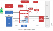
The PD chip CS32G052M of Xinhai Technology successfully passed the Thunderbolt 4 certification and entered the Intel Platform Component List (PCL) with its excellent product technical indicators and stable performance. This milestone achievement not only demonstrates the company's deep technical accumulation in the field of PD fast charging, but also marks the company's new breakthrough in the PC ecological layout.​

1717096716654.png

As we all know, Thunderbolt certification is regarded as the highest standard in the PD industry due to its complex and cumbersome certification process. It requires products to reach industry-leading levels in data transmission speed, power transmission efficiency, compatibility, etc. For a long time, this certification has been dominated and controlled by several internationally renowned manufacturers. With the passing of Thunderbolt certification by Chipsea Technology's CS32G052M and its entry into the Intel PCL list, it means that Chipsea's PD products have reached industry-leading standards in data transmission speed, stability, and compatibility.

CS32G052M is a single-channel USB Type-C and USB PD controller designed for laptops. It fully complies with the USB PD3.1 standard, supports single-channel independent fast charging, fully ensures charging speed and efficiency, and supports PPS function, which can bring users efficient and safe charging experience. In addition, CS32G052M has multiple protocol data transmission interfaces, supports many fast charging protocols, has a set of SBU Switch, a set of USB2.0 MUX, 12K SRAM and 256K Flash (supports dual-zone allocation), ensuring the stability and security of data transmission, and providing users with more flexible data transmission and control options.

Please, Log in or Register to view URLs content!
 

tokenanalyst

Brigadier
Registered Member

Microguide Nano intends to raise no more than 1.17 billion yuan to build an intelligent factory for semiconductor thin film deposition equipment​


Microguide Nano announced that it plans to issue convertible corporate bonds to unspecified objects with a total amount of funds raised not exceeding 1.17 billion yuan. After deducting the issuance costs, all funds will be invested in the construction of an intelligent factory for semiconductor thin film deposition equipment, the expansion of R&D laboratories, and the replenishment of working capital.

Microguide Nano is committed to the research of thin film deposition equipment. After years of development, it has formed a product system with atomic layer deposition (ALD) technology as the core and chemical vapor deposition (CVD) and other vacuum thin film technologies in a tiered development, covering multiple process technologies and product categories. At present, the company's products have covered logic, storage, new display (silicon-based OLED, etc.) and compound semiconductors and other fields.

The semiconductor thin film deposition equipment intelligent factory construction project that Microguide Nano intends to raise funds for is located in Xinwu District, Wuxi City, Jiangsu Province, with a total investment of 670 million yuan, and the amount of funds raised this time is planned to be 643 million yuan. The project plans to build an advanced production workshop, purchase advanced production equipment and measurement equipment, and enhance the company's production capacity of thin film deposition equipment.

Please, Log in or Register to view URLs content!
 

tokenanalyst

Brigadier
Registered Member

Aoxinming's first R&D center opened in Shanghai Lingang, and joined hands with ASMPT to draw a new blueprint for China's semiconductor back-end industry​


On May 27, the first R&D center of ASMPT Semiconductor Equipment Technology (Shanghai) Co., Ltd. opened in Lingang New Area. ASMPT is a local brand established by ASMPT to meet the needs of the Chinese market. With "advanced technology, empowering Chinese core" as the company's mission and slogan, it is committed to developing and providing domestic semiconductor packaging and testing equipment and solutions. The theme of the opening ceremony is "The future of Chinese core, Lingang starts a new journey", which means that domestic products based on ASMPT's advanced technology will take root in Lingang and promote the development of high-quality products in China's semiconductor industry. At the opening ceremony, Wu Xiaohua, deputy secretary of the Lingang New Area Party Working Committee, Yuan Tao, chairman of Zhangjiang Group, Huang Zida, CEO of ASMPT Group, and Xu Zhiwei, CEO of ASMPT, attended the ceremony. In addition, the heads of relevant departments such as the High-Tech Department, Financial Trade Department, and Party and Mass Department of the Management Committee also attended and witnessed this significant milestone.

Please, Log in or Register to view URLs content!
 

tokenanalyst

Brigadier
Registered Member

The Institute of Microelectronics published a review paper on new structure transistors for advanced CMOS integrated circuits in Science China: National Science Review​

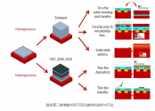
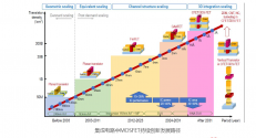
Metal-oxide-semiconductor field-effect transistors (MOSFETs) are the core devices that drive the continuous miniaturization and development of large-scale CMOS integrated circuits in accordance with "Moore's Law". In the past decade, in order to break through the miniaturization challenges at smaller technology nodes, transistor structure innovation has become the main path of technological development, from planar transistors to fin field-effect transistors, and then to the stacked nanochannel all-around gate FET (GAAFET) at the latest 3nm technology node, through the full three-dimensionalization of the internal channel of the transistor to obtain better short-channel gate control capabilities and the same size conductivity. Near the 1nm technology node, because the gate control capability of the MOSFET cannot be further improved and the internal Si-based conductive channel is close to the limit boundary of the carrier transmission quantum effect, the size reduction described by the traditional Moore's Law is no longer expected to be effective, and transistor structure innovation will move into a further vertical three-dimensional stacking of transistors.

1717099677989.png
Recently, the IC Pioneer Process R&D Team of the Institute of Microelectronics of the Chinese Academy of Sciences published a review article on new structure transistors for advanced technology node CMOS ICs online in the National Science Review (NSR) of the Chinese Science Magazine, and it was selected as the cover article of the journal. Starting from the key technical challenges faced by the latest GAAFET, the article introduces the main ways to achieve vertical three-dimensional stacking of transistors, including vertical complementary FETs (also known as 3D stacked FETs) and vertical channel transistors, in response to the integration density requirements of the continuous development of integrated circuits at the 1nm technology node. It summarizes the single and sequential integration paths and process methods for achieving three-dimensional stacking of transistors, the required innovative processes, materials (low-temperature epitaxial silicon, carbon nanotubes, two-dimensional materials, etc.) and collaborative design technologies, analyzes the key processes, circuit design and internal heat dissipation challenges for large-scale integrated applications, and looks forward to the comprehensive development possibilities of further integration with other new principle transistors and 3D chips and systems in the future.

Researcher Zhang Qingzhu and Senior Engineer Zhang Yongkui from the Institute of Microelectronics, Chinese Academy of Sciences are the first authors of the paper, and Researcher Yin Huaxiang is the corresponding author of the paper.

1717099724115.png

Please, Log in or Register to view URLs content!


SichuanHotPot

Banned Idiot
Registered Member
From listening to SMIC earnings call today

They definitely talked about need to build up capacity and the rationale for capex as being good for long term future of the company.
Talked about some customers gaining market share and needing rapid stocking up (interesting!!!)
7% increase in 8-inch equivalent shipment
3% decrease in ASP due to product mix
talked about focus on CIS, DDIC, High voltage, nor flash, nand flash, NVM, BCD platforms
While maintaining market share for medium to large screen, it has gained market share in small screens for smart phones & other consumer electronics
It has launched it's first 28nm DDIC for AMOLED screen
Received certification for CNSA for introduction of auto chip platform

12-inch product is "fully booked" as in it is facing bottleneck. Not seeing price declines there
pricing weakness is in 8-inch due to competition

SMIC getting increased market share in Chinese smartphones supply chain
28nm platform - need continued R&D
SMIC already produces what is referred to externally as 22nm (cut down version of 28nm)
SMIC produces this for DDIC, CIS, ISP, MCU & more (nand flash @ 24nm is a special version of 28nm product)
SMIC needs to continue to build the capacity here for its customers

Benefits from China for China movement

Talks about the role of running AI models on phones as a driver for chip advancements

continued to announce $7.5B capex this year, but who knows (they already spent $2.2B in Q1)

WOW,

At this rate, when will China become fully self-sufficient from 14 nm to 7 nm ?

My guess is 2 years. tphuang could you please comment ?
 

olalavn

Senior Member
Registered Member

Huawei and SMIC have a plan to produce 3nm chips​

It's quite possible that the U.S. sanctions that were intended to prevent Huawei from obtaining cutting-edge chips could fail. That's because Huawei filed a patent to use self-aligned quadruple patterning (SAQP) lithography to build 3nm chips using multi-patterning techniques. The multi-patterning techniques are the subject of another patent filed by state-funded chip manufacturing company SiCarrier which, according to Tom's Hardware, confirms that China's largest foundry SMIC is interested in using SAQP to produce 3nm chips for Huawei using Deep Ultraviolet (DUV) lithography machines.
Please, Log in or Register to view URLs content!
Currently, Huawei only has 7nm technology, we don't have 5nm or 3nm technology... but the transistor level of the 7nm chip is very strange....


1717116074186.png
 

Phead128

Captain
Staff member
Moderator - World Affairs

Huawei and SMIC have a plan to produce 3nm chips​

It's quite possible that the U.S. sanctions that were intended to prevent Huawei from obtaining cutting-edge chips could fail.
"But but we have 1.6nm nodes on the way! Ergo, sanctions working as intended."
- Gina et al.

US sanctions was aimed at achieving 0% yield at 14nm/16nm and below (i.e. "advanced logic"), ergo, sanctions are not working if China achieves 7nm/5nm/3nm at >0% yield. They are by definition ineffective sanctions. For the "at what cost-ing" pundits, the extra cost of 5nm/3nm can be subsidized at cheaper rate than a single Israel or Ukraine aid package.
 
Last edited:

SichuanHotPot

Banned Idiot
Registered Member
China's saw IC production increase by 31.9% YoY in April

so far this year, it is up 37.2%

Unreal !

Just wondering, how much can China replace imports by the end of this year ?

I heard that China imported 400 billion $ worth of chips in 2022 more than oil, how much has it dropped ?
 

Hyper

Junior Member
Registered Member
Top