Chinese semiconductor thread II

tokenanalyst

Brigadier
Registered Member

Zhuhai Chip-Mills achieves 28nm FPGA tape-out​

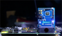
Zhuhai Zuixin Semiconductor Co., Ltd. disclosed that it had recently successfully achieved 28-nanometer tape-out. The Zuixin CERES-1FPGA chip is benchmarked against the 28-nanometer FPGA international mainstream architecture, achieving pin compatibility and bitstream compatibility. With the Zuixin KUIPER-1 development board, users can seamlessly connect to the international mainstream development platform and ecosystem, and realize the domestic substitution of chips and development boards.

According to reports, CERES-1 FPGA contains 600,000 logic gates, 3,750 6-input logic lookup tables, 100 user IOs, 180KB on-chip storage, and 10 DSP units. The MPW tape-out successfully verified the maturity and reliability of Zhuhai Zuanxin's 28nm FPGA technology. The next milestone for Zhuhai Zuanxin is the mass production of 28nm FPGA chips.

Please, Log in or Register to view URLs content!
 

GulfLander

Captain
Registered Member
BEIJING, May 30 (Xinhua) -- A group of Chinese scientists have pioneered the creation of the world's first brain-inspired complementary vision chip, endowing machines with a human-like visual perception capability.
1717058787164.png
Chinese scientists have developed the world's first vision chip with complementary pathways for open-world sensing, achieving high-speed sensing of up to 10,000 fps and a dynamic range of 130 dB, despite a 90% reduction in bandwidth.

Please, Log in or Register to view URLs content!
 

test1979

Junior Member
Registered Member

Huawei and SMIC have a plan to produce 3nm chips​

It's quite possible that the U.S. sanctions that were intended to prevent Huawei from obtaining cutting-edge chips could fail. That's because Huawei filed a patent to use self-aligned quadruple patterning (SAQP) lithography to build 3nm chips using multi-patterning techniques. The multi-patterning techniques are the subject of another patent filed by state-funded chip manufacturing company SiCarrier which, according to Tom's Hardware, confirms that China's largest foundry SMIC is interested in using SAQP to produce 3nm chips for Huawei using Deep Ultraviolet (DUV) lithography machines.
Please, Log in or Register to view URLs content!
 

measuredingabens

Junior Member
Registered Member

Huawei and SMIC have a plan to produce 3nm chips​

It's quite possible that the U.S. sanctions that were intended to prevent Huawei from obtaining cutting-edge chips could fail. That's because Huawei filed a patent to use self-aligned quadruple patterning (SAQP) lithography to build 3nm chips using multi-patterning techniques. The multi-patterning techniques are the subject of another patent filed by state-funded chip manufacturing company SiCarrier which, according to Tom's Hardware, confirms that China's largest foundry SMIC is interested in using SAQP to produce 3nm chips for Huawei using Deep Ultraviolet (DUV) lithography machines.
Please, Log in or Register to view URLs content!
I'm fairly certain this was the same patent SiCarrier filed a month ago.
Chinese semiconductor thread II
 

tphuang

Lieutenant General
Staff member
Super Moderator
VIP Professional
Registered Member
W/ Sanan entering Europe, does that mean China SiC MOSFET demand outside of BYD is not enough to fill the Changsha 12k wpm fab? Wonder what this will mean for MOSFET pricing when they ramp to 40k wpm and won't this be in direct competition with their JV w/ STM?
i don't think you need to overthink this. Just because they enter Europe, doesn't mean they are not also expanding their relationships in China. You can supply many regions at the same time
 

tokenanalyst

Brigadier
Registered Member

The Institute of Metal Research, Chinese Academy of Sciences, has made important breakthroughs in the research of two-dimensional semiconductor devices​


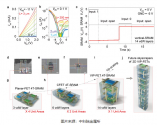
Information from the Institute of Metal Research, Chinese Academy of Sciences shows that under the leadership of Professor Han Zheng of Shanxi University, a collaboration involving Researcher Li Xiuyan from the Institute of Metal Research, Chinese Academy of Sciences, Associate Researcher Wang Hanwen from Liaoning Materials Laboratory, Professor Hou Yanglong from Sun Yat-sen University, and Professor Zhou Wu from University of Chinese Academy of Sciences has proposed a new p-doped two-dimensional semiconductor method based on interface coupling (theory shows that quantum effects play a key role in this), providing ideas for the development of future two-dimensional semiconductor devices in the post-Moore era.

As semiconductor process technology continues to approach the sub-nanometer physical limit, developing a vertically structured multi-layer interconnected CMOS logic circuit to achieve a breakthrough in three-dimensional integration technology is one of the new paths actively explored in the international semiconductor field. Since the silicon-based transistor preparation process uses ion implantation on the surface of single-crystal silicon, it is difficult to grow or transfer single-crystal silicon again on top of a layer of ion-implanted single-crystal silicon. Although the integration level can be improved by connecting electrodes and core particles in three-dimensional space, the key transistors are always distributed at the bottom layer and cannot obtain the degree of freedom in the z direction. New materials or disruptive principles have therefore become important breakthroughs that have attracted much attention.

1717075817807.png

Please, Log in or Register to view URLs content!
 

measuredingabens

Junior Member
Registered Member

The Institute of Metal Research, Chinese Academy of Sciences, has made important breakthroughs in the research of two-dimensional semiconductor devices​


Information from the Institute of Metal Research, Chinese Academy of Sciences shows that under the leadership of Professor Han Zheng of Shanxi University, a collaboration involving Researcher Li Xiuyan from the Institute of Metal Research, Chinese Academy of Sciences, Associate Researcher Wang Hanwen from Liaoning Materials Laboratory, Professor Hou Yanglong from Sun Yat-sen University, and Professor Zhou Wu from University of Chinese Academy of Sciences has proposed a new p-doped two-dimensional semiconductor method based on interface coupling (theory shows that quantum effects play a key role in this), providing ideas for the development of future two-dimensional semiconductor devices in the post-Moore era.

As semiconductor process technology continues to approach the sub-nanometer physical limit, developing a vertically structured multi-layer interconnected CMOS logic circuit to achieve a breakthrough in three-dimensional integration technology is one of the new paths actively explored in the international semiconductor field. Since the silicon-based transistor preparation process uses ion implantation on the surface of single-crystal silicon, it is difficult to grow or transfer single-crystal silicon again on top of a layer of ion-implanted single-crystal silicon. Although the integration level can be improved by connecting electrodes and core particles in three-dimensional space, the key transistors are always distributed at the bottom layer and cannot obtain the degree of freedom in the z direction. New materials or disruptive principles have therefore become important breakthroughs that have attracted much attention.

View attachment 130326

Please, Log in or Register to view URLs content!
Here's the paper for anyone interested.
Please, Log in or Register to view URLs content!

Van der Waals polarity-engineered 3D integration of 2D complementary logic​

Abstract​

Vertical three-dimensional integration of two-dimensional (2D) semiconductors holds great promise, as it offers the possibility to scale up logic layers in the z axis
Please, Log in or Register to view URLs content!
,
Please, Log in or Register to view URLs content!
,
Please, Log in or Register to view URLs content!
. Indeed, vertical complementary field-effect transistors (CFETs) built with such mixed-dimensional heterostructures
Please, Log in or Register to view URLs content!
,
Please, Log in or Register to view URLs content!
, as well as hetero-2D layers with different carrier types
Please, Log in or Register to view URLs content!
,
Please, Log in or Register to view URLs content!
,
Please, Log in or Register to view URLs content!
, have been demonstrated recently. However, so far, the lack of a controllable doping scheme (especially p-doped WSe2 (refs.
Please, Log in or Register to view URLs content!
,
Please, Log in or Register to view URLs content!
,
Please, Log in or Register to view URLs content!
,
Please, Log in or Register to view URLs content!
,
Please, Log in or Register to view URLs content!
,
Please, Log in or Register to view URLs content!
,
Please, Log in or Register to view URLs content!
,
Please, Log in or Register to view URLs content!
,
Please, Log in or Register to view URLs content!
) and MoS2 (refs.
Please, Log in or Register to view URLs content!
,
Please, Log in or Register to view URLs content!
,
Please, Log in or Register to view URLs content!
,
Please, Log in or Register to view URLs content!
,
Please, Log in or Register to view URLs content!
,
Please, Log in or Register to view URLs content!
,
Please, Log in or Register to view URLs content!
,
Please, Log in or Register to view URLs content!
,
Please, Log in or Register to view URLs content!
,
Please, Log in or Register to view URLs content!
,
Please, Log in or Register to view URLs content!
,
Please, Log in or Register to view URLs content!
)) in 2D semiconductors, preferably in a stable and non-destructive manner, has greatly impeded the bottom-up scaling of complementary logic circuitries. Here we show that, by bringing transition metal dichalcogenides, such as MoS2, atop a van der Waals (vdW) antiferromagnetic insulator chromium oxychloride (CrOCl), the carrier polarity in MoS2 can be readily reconfigured from n- to p-type via strong vdW interfacial coupling. The consequential band alignment yields transistors with room-temperature hole mobilities up to approximately 425 cm2 V−1 s−1, on/off ratios reaching 106 and air-stable performance for over one year. Based on this approach, vertically constructed complementary logic, including inverters with 6 vdW layers, NANDs with 14 vdW layers and SRAMs with 14 vdW layers, are further demonstrated. Our findings of polarity-engineered p- and n-type 2D semiconductor channels with and without vdW intercalation are robust and universal to various materials and thus may throw light on future three-dimensional vertically integrated circuits based on 2D logic gates.
 
Top