Semiwiki states that DUV SAQP means that such a process restricts design flexibility so the node is probably tailore made for Huawei. 90% of the wafers are for Huawei.Additional info form the video:
of Kirin 9010 is 10.738 x 10.879 = 116.8187mm^2 ->
of Kirin 9000S is 10.39x10.65 = 110.6535mm^2 -> 540 dies/wafer
The 2 Kirin chips , mainly due to increase L2/L3 cache. The other modules are the same.
with Snapdragon sizes.
Regarding the 9010, we don't know the yield nor the current capacity, but we can calculate backward what it would take to cover 60M phones per year.
For 60M phones per year, at a capacity of 15K wpm (not all SMIC capacity goes into the Kirin) it is enough a minimum yield of 65%
....but we can expect actual yield should be al least 70% and possibly even higher than 80%.
Dedicated SMIC capacity 15Kwpm
yield phones per year 65% 60M 76% 70M 87% 80M
Dedicated SMIC capacity 20Kwpm
yield phones per year 65% 80M 76% 93M 87% 106M
You are using an out of date browser. It may not display this or other websites correctly.
You should upgrade or use an alternative browser.
You should upgrade or use an alternative browser.
Chinese semiconductor thread II
- Thread starter vincent
- Start date
What is the current SMIC 7nm capacity? Iinm it's like 20k wpm right?Additional info form the video:
of Kirin 9010 is 10.738 x 10.879 = 116.8187mm^2 ->
of Kirin 9000S is 10.39x10.65 = 110.6535mm^2 -> 540 dies/wafer
The 2 Kirin chips , mainly due to increase L2/L3 cache. The other modules are the same.
with Snapdragon sizes.
Regarding the 9010, we don't know the yield nor the current capacity, but we can calculate backward what it would take to cover 60M phones per year.
For 60M phones per year, at a capacity of 15K wpm (not all SMIC capacity goes into the Kirin) it is enough a minimum yield of 65%
....but we can expect actual yield should be al least 70% and possibly even higher than 80%.
Dedicated SMIC capacity 15Kwpm
yield phones per year 65% 60M 76% 70M 87% 80M
Dedicated SMIC capacity 20Kwpm
yield phones per year 65% 80M 76% 93M 87% 106M
Also, are there any plans to develop an alternative supplier to Huawei? Basically like how US forced Intel to cultivate AMD as an alternative.
antiterror13
Brigadier
10 micron is 0.00001m or roughly 1/7 of human hair diameter, pretty thinMore intersection of radar industry and semi here
this lady is award price for
engineering development and production of the first 10-micron gold wire bonding TR component in China. says she is involved in land, sea, air & space type of radar
just looking at this page here
it mentions 18 to 50 micron diameter gold wire bonding.
This one here says they can do up to 15 micron for very fine application
So 10 micron is pretty world class.
It seems to me that thinner gold wire bonding would be important here in miniaturization.
as for why gold
Seems like it's ability to withstand harsh temperature, which is needed for weapon system
Wondering how many gram is for 1km of the 10 micron gold wire ?
19.32 x (Pi x 0.25 x (0.00001)^2) x 1,000 x 1000 x 1000 = 1.5 grms .... really? what I did wrong?
first 1,000 is for 1 kms to meter
The second and third 1,000 is to kg and gr
Last edited:
HCUT is committed to 100% localization of core components of semiconductor equipment.
Founded in 2020 and located in Wujiang Development Zone, Gaoxin Zhongke is a high-tech enterprise in the pan-semiconductor industry. It focuses on the innovative application of special high-end coating technologies and the research and development and manufacturing of related materials, and is committed to truly achieving 100% localization of core components of semiconductor equipment.
Although semiconductor equipment is everywhere, the "gold content" represented by the word "semiconductor" and "chip" is often accompanied by words such as "blockade" and "choke point". There is even a topic that has been discussed for several years on the Zhihu forum: which is more difficult, making an atomic bomb or making a semiconductor chip? It can be seen that the research and development and production of semiconductor materials are difficult. Under the leadership of Chairman Xin Changlin, Gaoxin Zhongke is such a semiconductor component and related material research and development and production enterprise that dares to bite the "hard bone" and break the "ceiling" . It is committed to unlocking the "core" power of high-quality development with new quality productivity and promoting the high-end development of China's semiconductor industry.
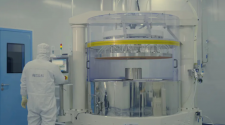
Since he started his business in 2015 and entered the semiconductor core parts market, Xin Changlin has set his sights on high-tech semiconductor special coatings and related materials, electrodes and other core parts, focusing on the production and development of ceramic materials and the production of ceramic parts. The R&D team launched the first semiconductor product after four years of continuous efforts. In Xin Changlin's own words, this process was "unbearable to look back on, and I almost couldn't hold on."
From glass to screens, from silicon wafers to chips, due to the complexity and severity of the manufacturing process, they generally need to be carried out in a vacuum environment. This is also the semiconductor vacuum chamber component, one of the core products of Gochip. The completion of such products not only requires high processing technology, but also involves special coatings and related materials, which makes people who do not understand or are not proficient in this industry discouraged. However, Xin Changlin believes that there is no problem that cannot be solved.
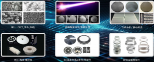
Founded in 2020 and located in Wujiang Development Zone, Gaoxin Zhongke is a high-tech enterprise in the pan-semiconductor industry. It focuses on the innovative application of special high-end coating technologies and the research and development and manufacturing of related materials, and is committed to truly achieving 100% localization of core components of semiconductor equipment.
Although semiconductor equipment is everywhere, the "gold content" represented by the word "semiconductor" and "chip" is often accompanied by words such as "blockade" and "choke point". There is even a topic that has been discussed for several years on the Zhihu forum: which is more difficult, making an atomic bomb or making a semiconductor chip? It can be seen that the research and development and production of semiconductor materials are difficult. Under the leadership of Chairman Xin Changlin, Gaoxin Zhongke is such a semiconductor component and related material research and development and production enterprise that dares to bite the "hard bone" and break the "ceiling" . It is committed to unlocking the "core" power of high-quality development with new quality productivity and promoting the high-end development of China's semiconductor industry.

Since he started his business in 2015 and entered the semiconductor core parts market, Xin Changlin has set his sights on high-tech semiconductor special coatings and related materials, electrodes and other core parts, focusing on the production and development of ceramic materials and the production of ceramic parts. The R&D team launched the first semiconductor product after four years of continuous efforts. In Xin Changlin's own words, this process was "unbearable to look back on, and I almost couldn't hold on."
From glass to screens, from silicon wafers to chips, due to the complexity and severity of the manufacturing process, they generally need to be carried out in a vacuum environment. This is also the semiconductor vacuum chamber component, one of the core products of Gochip. The completion of such products not only requires high processing technology, but also involves special coatings and related materials, which makes people who do not understand or are not proficient in this industry discouraged. However, Xin Changlin believes that there is no problem that cannot be solved.

Tongjia Hongrui Technology completed its B round of financing and is a supplier of dry vacuum pump equipment for the semiconductor industry
Tongjia Hongrui Technology has recently completed its B round of financing. The co-investors in this round include Qingsong Capital, Fortune Capital, and China Development Bank Science and Technology Innovation.
Tongjia Technology was founded in 2012 and is headquartered in Beijing. According to Qingsong Capital, Beijing Tongjia Hongrui Technology Co., Ltd. is a high-tech enterprise focusing on the research and development, production, sales and service of high-end semiconductor-grade dry vacuum pumps. It is a global supplier of dry vacuum pump equipment and system technology services for the semiconductor industry.
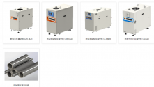
The company's main business is "semiconductor-grade vacuum pumps and vacuum pump maintenance, cleaning services and sales of supporting core components close to major customers". Its leading products are a full range of international mainstream dry vacuum pumps and core precision components, which are widely used in integrated circuits, etching, vacuum film and other equipment in the semiconductor, display panel, solar photovoltaic, LED lighting, lithium battery and other industries. It has won the attention of the industry with its core competitive advantages such as high efficiency, energy saving, environmental protection, high cost performance and adaptability to harsh working conditions.
Tongjia Technology was founded in 2012 and is headquartered in Beijing. According to Qingsong Capital, Beijing Tongjia Hongrui Technology Co., Ltd. is a high-tech enterprise focusing on the research and development, production, sales and service of high-end semiconductor-grade dry vacuum pumps. It is a global supplier of dry vacuum pump equipment and system technology services for the semiconductor industry.

The company's main business is "semiconductor-grade vacuum pumps and vacuum pump maintenance, cleaning services and sales of supporting core components close to major customers". Its leading products are a full range of international mainstream dry vacuum pumps and core precision components, which are widely used in integrated circuits, etching, vacuum film and other equipment in the semiconductor, display panel, solar photovoltaic, LED lighting, lithium battery and other industries. It has won the attention of the industry with its core competitive advantages such as high efficiency, energy saving, environmental protection, high cost performance and adaptability to harsh working conditions.
And how exactly can they do that?Looks like there is another group of companies that are slowly crawling up creating a sort of secondary supply chain for semiconductor optical lithography apart from the establish companies of the project 02.
I have seen new companies in:
- High end wafer precision motion.
- High end lithography optics.
- High end positioning sensing.
- High end excimer light sources.
View attachment 130410
This companies for now are serving other sectors like metrology equipment and so on but there is a possibility that we are going to see DUV scanners from other company apart from SMEE and ASML and others in China.
In that case my guess is that ASML and Nikon may use their patent portfolio to try to stop any company in China apart from SMEE from developing DUV lithography machines so they don't have so many competitors cabbagetizating the lithography industry.
By going after enforcing their patents against smaller companies that does not have the state backup that SMEE have. Instead of going after U-Precision they could go after Yinguan Semiconductor if they develop similar products.And how exactly can they do that?
The third-generation semiconductor industry in Zhongguancun Shunyi Park has achieved new breakthroughs!
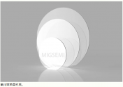
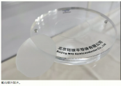
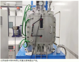
According to Chen Zhengwei, chairman of Beijing Mingga Semiconductor Co., Ltd., the semi-insulating (010) iron-doped substrate and the substrate plus conductive thin film epitaxy can currently be made to 25 mm × 25 mm in size internationally, while Mingga Semiconductor can make it to 40 mm × 25 mm, and can stably produce multiple furnaces and accumulate a certain amount of inventory. The conductive (001) tin-doped substrate and the substrate plus conductive thin film epitaxy can currently reach 4 inches internationally. Mingga Semiconductor has achieved a breakthrough in large-size substrate technology and will gradually stabilize the process supply.

The Indian origin woman behind the US tech sanctions:
Key quote:
“When I do travel — and by overseas l mean Taiwan, Japan, Korea, Switzerland, Germany, the Netherlands, U.K., you know, allied countries — almost to a person, they don’t really understand what the national security objective is that the U.S. government is trying to accomplish with all these new controls,” said Wolf, the former assistant commerce secretary.
Some, such as Atkinson, say the grants for building new U.S. technological hubs have been distributed too diffusely.
“The whole point of this was you can’t have 50 places,” he said. “There’s not enough money. There’s not enough technology to go around.”
Another interesting article:
Key paragraph:
Will a successful implementation of the four above measures remove the threat of China’s control over certain global supply chains? No. It will only buy time for the West. If everything goes well with implementation, it will increase the production capacity of the Western economies in the chips sector. But then to whom will these newly added mature chips be sold given that these economies are overwhelmingly de-industrialized? Perhaps again to China, where local industry still grows steadily. Currently, this is the case with the US corporation Applied Materials, which makes about 45% of its revenue from China and will probably lose it like other similar big producers in the West if the latter invests more into mature chips.
Last edited:
