Chinese semiconductor thread II

curiouscat

Junior Member
Registered Member
Please, Log in or Register to view URLs content!

It would be interesting to read this article from Digitimes.
Please, Log in or Register to view URLs content!

Huawei chip development receives all-out support from Chinese semiconductor firms​

Monica Chen, Taipei; Rodney Chan, DIGITIMES AsiaTuesday 14 May 2024
Please, Log in or Register to view URLs content!


1_b.jpg

Credit: AFP

Huawei has recently launched its Pura 70 series smartphones featuring its in-house developed Kirin 9010 application processors made using SMIC's 7nm N+2 manufacturing process.
Huawei's chip development has been receiving strong support from local semiconductor firms – all acting in line with China's bid to improve the country's chip self-sufficiency at all costs, according to sources from Taiwan's fab tool supply chain. Apart from SMIC, which provides wafer foundry support, Huawei has been backed by another foundry house JHICC, and packaging and testing firms Tongfu Microelectronics and SJ Semiconductor, the sources said.
US sanctions have dealt a heavy blow to Huawei over the past few years. Its quarterly net income fell from CNY14.38 billion (US$1.99 billion) in the first quarter of 2019, to CNY13.3 billion in the first quarter of 2020, and further to only CNY3.04 billion in the first quarter of 2023.
But Huawei has reported a strong rebound for its first-quarter 2024 finances, with sales coming to CNY178.45 billion and net income soaring 564% year-on-year to reach CNY19.65 billion. It is the best quarterly results that Huawei has reported since the US hit it with sanctions. It shows that Huawei has now found a way to circumvent the US ban and move its handset and networking equipment businesses back on track, the sources said.
The sources said Huawei's strong rebound is due to all-out support from the Chinese government and local semiconductor firms.
Please, Log in or Register to view URLs content!
, the sources added.
China's advanced chip manufacturing has been hit by a US export ban on EUV tools to the country. Instead, SMIC has employed DUV tools to advance to 7nm manufacturing for making Huawei's handset chips.

SMIC incurs high costs making 7nm chips​

Burn-Jeng Lin, former TSMC VP of R&D, has pointed out that the Taiwanese foundry house can make 7nm chips using DUV technology. SMIC certainly can also do it, but the cost will be very high, he said. Using DUV tools to make 5nm chips will incur even higher costs, with low yield rates, Lin said.
But SMIC is spending big on constructing advanced manufacturing capacity to mainly support Huawei. After yield rates are improved and costs reduced, SMIC will expand its reach to other Chinese customers, the sources said.
Please, Log in or Register to view URLs content!
JHICC, which came under US sanctions a few years ago, has started making chips for Huawei. With strong demand from Huawei and its chip design arm HiSilicon, JHICC has been expanding its wafer fab capacity, the sources said.
Tongfu and SJ Semiconductor are also providing Huawei with packaging technology support for advancing its chips, the sources said.

Advanced packaging crucial for Huawei​

Huawei chairman Guo Ping has pointed out that advanced packaging is crucial to Huawei breaking the stranglehold. Tongfu is a major player in the world's semiconductor backend sector, with production bases in China and Malaysia.
In 2016, with support from China's Big Fund, Tongfu acquired majority stakes in AMD's plants in China's Suzhou and Malaysia's Penang. It has also formed a packaging and testing joint-venture firm with AMD. The US chip vendor is the biggest customer for Tongfu.
The partnership with AMD has helped enhance Tongfu's technological prowess, the sources said, adding that Tongfu will see the proportion of orders from Huawei grow.
SJ Semiconductor, founded in 2014, offers 12-inch bumping, WLCSP, and testing services. It has also entered the 3DIC sector, and has been devoting a lot of resources to developing CoWoS technology, the sources said. SJ Semiconductor is rising fast in China's backend sector, and is also tasked with helping Huawei break the US stranglehold, the sources said.

Looks like Huawei is not only sourcing chips from SMIC but has also started sourcing them from JHICC now as well. Also, lots of ongoing work on advanced packaging.
 

vincent

Grumpy Old Man
Staff member
Moderator - World Affairs
US and Europe will defend their advanced industries at any cost, because to have an edge in technology is what allowed the West to be "The West" from the industrial revolution 3 centuries ago untill today.

So we will have more of this, for sure.
The West can keep their markets to themselves while China has the rest of the world.
 

Wahid145

Junior Member
Registered Member
Please, Log in or Register to view URLs content!

Huawei chip development receives all-out support from Chinese semiconductor firms​

Monica Chen, Taipei; Rodney Chan, DIGITIMES AsiaTuesday 14 May 2024
Please, Log in or Register to view URLs content!


1_b.jpg

Credit: AFP

Huawei has recently launched its Pura 70 series smartphones featuring its in-house developed Kirin 9010 application processors made using SMIC's 7nm N+2 manufacturing process.
Huawei's chip development has been receiving strong support from local semiconductor firms – all acting in line with China's bid to improve the country's chip self-sufficiency at all costs, according to sources from Taiwan's fab tool supply chain. Apart from SMIC, which provides wafer foundry support, Huawei has been backed by another foundry house JHICC, and packaging and testing firms Tongfu Microelectronics and SJ Semiconductor, the sources said.
US sanctions have dealt a heavy blow to Huawei over the past few years. Its quarterly net income fell from CNY14.38 billion (US$1.99 billion) in the first quarter of 2019, to CNY13.3 billion in the first quarter of 2020, and further to only CNY3.04 billion in the first quarter of 2023.
But Huawei has reported a strong rebound for its first-quarter 2024 finances, with sales coming to CNY178.45 billion and net income soaring 564% year-on-year to reach CNY19.65 billion. It is the best quarterly results that Huawei has reported since the US hit it with sanctions. It shows that Huawei has now found a way to circumvent the US ban and move its handset and networking equipment businesses back on track, the sources said.
The sources said Huawei's strong rebound is due to all-out support from the Chinese government and local semiconductor firms.
Please, Log in or Register to view URLs content!
, the sources added.
China's advanced chip manufacturing has been hit by a US export ban on EUV tools to the country. Instead, SMIC has employed DUV tools to advance to 7nm manufacturing for making Huawei's handset chips.

SMIC incurs high costs making 7nm chips​

Burn-Jeng Lin, former TSMC VP of R&D, has pointed out that the Taiwanese foundry house can make 7nm chips using DUV technology. SMIC certainly can also do it, but the cost will be very high, he said. Using DUV tools to make 5nm chips will incur even higher costs, with low yield rates, Lin said.
But SMIC is spending big on constructing advanced manufacturing capacity to mainly support Huawei. After yield rates are improved and costs reduced, SMIC will expand its reach to other Chinese customers, the sources said.
Please, Log in or Register to view URLs content!
JHICC, which came under US sanctions a few years ago, has started making chips for Huawei. With strong demand from Huawei and its chip design arm HiSilicon, JHICC has been expanding its wafer fab capacity, the sources said.
Tongfu and SJ Semiconductor are also providing Huawei with packaging technology support for advancing its chips, the sources said.

Advanced packaging crucial for Huawei​

Huawei chairman Guo Ping has pointed out that advanced packaging is crucial to Huawei breaking the stranglehold. Tongfu is a major player in the world's semiconductor backend sector, with production bases in China and Malaysia.
In 2016, with support from China's Big Fund, Tongfu acquired majority stakes in AMD's plants in China's Suzhou and Malaysia's Penang. It has also formed a packaging and testing joint-venture firm with AMD. The US chip vendor is the biggest customer for Tongfu.
The partnership with AMD has helped enhance Tongfu's technological prowess, the sources said, adding that Tongfu will see the proportion of orders from Huawei grow.
SJ Semiconductor, founded in 2014, offers 12-inch bumping, WLCSP, and testing services. It has also entered the 3DIC sector, and has been devoting a lot of resources to developing CoWoS technology, the sources said. SJ Semiconductor is rising fast in China's backend sector, and is also tasked with helping Huawei break the US stranglehold, the sources said.

Looks like Huawei is not only sourcing chips from SMIC but has also started sourcing them from JHICC now as well. Also, lots of ongoing work on advanced packaging.
Yup! I'm curious whats JHICC is making for them. I know Huawei has been working with JHICC for a long time and before the American government sanctioned them they were like CXMT venturing into the DRAM sector
 

proelite

Junior Member
What kind of manufacturing does the US do that needs mature semiconductors from China? The ones that do can easily pass on the costs to the customers, we're talking about cents added in costs.

Seems like the both the EV and semi-tariffs are political gestures.
 

tokenanalyst

Brigadier
Registered Member

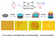
Zhejiang University researchers have made progress in creating water-developable photoresist​


With funding from the National Natural Science Foundation of China (Grant No. T2225004) and other projects, Professor Wu Guangpeng’s team from Zhejiang University has made new progress in the creation of chemical amplification photoresists. The relevant research results include "water-developable high-performance carbon dioxide-based chemical amplification photoresist". "Aqueous Developable and CO2-Sourced Chemical Amplification Photoresist with High Performance" was published in Angewandte Chemie International Edition on May 5.
1715719556138.png


Chemically amplified photoresist is currently the most widely used photolithography material in integrated circuit manufacturing. By constructing a photoacid-catalyzed acidolysis reaction, the sensitivity of the photoresist can be improved by orders of magnitude, making up for the efficiency problems caused by the decrease in light source power of the lithography machine. As the critical dimensions of chips continue to be miniaturized, the development of high-performance photoresist has become an indispensable technical link in chip manufacturing. Carbonate and acetal groups are important acid-sensitive structural units in traditional chemical amplification photoresists. However, due to too low acid decomposition activation energy, such photoresists are prone to self-development during the photolithography process, resulting in Volatile substances can easily contaminate the lens of the photolithography machine. At the same time, traditional chemically amplified photoresists use tetramethylammonium hydroxide solution as the developer, which can easily cause poisoning and environmental problems. In addition, this type of photoresist system is also prone to dark reactions during placement, affecting storage and photolithography stability. In response to the above challenges and problems, the team of Professor Wu Guangpeng of Zhejiang University used a self-developed highly active organoboron catalyst and used carbon dioxide and an epoxy compound with an acid-sensitive cyclic acetal structure as raw materials to prepare a carbonate-based main product with high transparency. A new photoresist film-forming resin with chain and highly acid-sensitive acetal side groups.

Under the condition of deep ultraviolet light exposure, the acetal group in the photoacid catalyzed resin undergoes a hydrolysis reaction, causing the film-forming resin to undergo a hydrophilic and hydrophobic transition, thereby enabling direct development with water. The author compared the performance of the prepared photoresist resin with commercial KrF and ArF photoresist resins. The results show that this type of chemically amplified photoresist exhibits excellent comprehensive properties such as sensitivity, contrast, resolution and etching resistance. At the same time, this type of photoresist system can be stored stably for more than 60 days at room temperature and has good stability.

In short, this work designed and synthesized a type of water-developable deep ultraviolet chemically amplified photoresist film-forming resin. The photolithography mechanism of this system was explored and excellent photolithography performance was achieved. It provides a basis for the development of high-performance deep ultraviolet and Extreme ultraviolet photoresist provides a new idea.​
 

tokenanalyst

Brigadier
Registered Member

Luwei Optoelectronics: Q1 mask revenue has increased significantly and procurement costs are expected to be optimized.​


As an upstream mask provider in the display and semiconductor industry chain, Luwei Optoelectronics' performance in 2023 and the first quarter of this year continues to improve. In 2023, the company achieved revenue of 672 million yuan, a year-on-year increase of 5.06%; net profit attributable to the parent company was 149 million yuan, a year-on-year increase of 24.23%. Revenue in the first quarter of this year was 177 million yuan, a year-on-year increase of 30.10%; net profit attributable to the parent company was 41.07 million yuan, a year-on-year increase of 59.16%.

Du Wubing said at today's (May 9) performance meeting that with the help of the release of new semiconductor factory capacity around the world and the massive construction of new semiconductor manufacturing plants, the overall market demand for masks for semiconductor chips is expected to continue to grow. And provide strong support for the recovery and development of the semiconductor industry. "Taken together, the market demand for masks continues to increase."

In terms of semiconductor applications, Luwei Optoelectronics has achieved mass production of semiconductor masks for 180nm process nodes and above, and has formed core technologies for mature processes at 150nm process nodes and below. Its products are widely used in MOSFET, IGBT, MEMS, SAW, advanced packaging, etc. Semiconductor manufacturing field, and covering third generation semiconductor related products. In terms of downstream customers, the company has established cooperative relationships with some of the country's leading chip companies and their supporting suppliers, as well as SMIC Ningbo, Tongfu Microelectronics, Jingfang Technology, Huatian Technology and many other mainstream domestic manufacturers.

Luwei Optoelectronics continued to deploy cutting-edge semiconductor technologies and improve its industrial chain cooperation through foreign investment last year. In 2023, the company used its own funds to jointly launch the industrial fund Luvis Shengde with Shenzhen Qianhai Ruixing Investment Management Co., Ltd. and completed two industrial investments, including an indirect investment of 160 million yuan in Jiangsu Luxin Semiconductor Technology Co., Ltd. The company's 130nm-28nm process node semiconductor mask production line project is expected to have a total investment of 2 billion yuan, and it will subscribe for approximately 7.04 million shares of Hunan Puzhao Information Materials Co., Ltd. for 10 million yuan.


tokenanalyst

Brigadier
Registered Member

vivo X100 Ultra is first equipped with domestic ultrasonic fingerprint solution​

Vivo released its new imaging flagship phone X100 Ultra, priced from 6,499 yuan. It is equipped with a one-inch gimbal-level main camera and Zeiss 200-megapixel APO super telephoto, priced at 6,499 yuan to 7,999 yuan.
Currently, vivo X100 series mobile phones have 5 products, namely: X100 and X100 Pro equipped with Dimensity 9300 chip; X100s and X100s Pro equipped with Dimensity 9300+ chip; X100 Ultra equipped with Snapdragon 8 Gen3 chip.
It is reported that the X100 Ultra mobile phone is the first to use the ultrasonic fingerprint recognition solution independently developed by domestic brand Goodix Technology. At present, mainstream smartphones mostly use optical fingerprint recognition solutions, which have a slower response and lower recognition rate than ultrasonic recognition. The optical fingerprint recognition components are thicker, resulting in a limited recognition area and inconvenience for users to operate. According to the official introduction, the new ultrasonic fingerprint solution equipped with vivo X100 Ultra has better signal-to-noise ratio, can obtain clearer fingerprint images, supports second-speed recognition, and can unlock in one go even with oily or wet fingers; it uses ultrasonic waves to sense user fingerprints Three-dimensional features such as valleys and ridges are used to construct an accurate 3D fingerprint "map", making fingerprint recognition more secure.

Please, Log in or Register to view URLs content!
 

mst

Junior Member
Registered Member
Please, Log in or Register to view URLs content!

Two Chinese chipmakers are in the early stages of producing high bandwidth memory (HBM) semiconductors used in artificial intelligence chipsets, according to sources and documents.

The progress in HBM - even if only in older versions of HBM - represents a major step forward in China's efforts to reduce its reliance on foreign suppliers amid tensions with Washington that have led to restrictions on U.S. exports of advanced chipsets to Chinese firms.

CXMT, China's top manufacturer of DRAM chips, has developed sample HBM chips in partnership with chip packaging and testing company Tongfu Microelectronics, according to three people briefed on the matter. The chips are being shown to clients, two of them said.

In another example, Wuhan Xinxin is building a factory that will be able to produce 3,000 12-inch HBM wafers a month with construction slated to have begun in February this year, documents from corporate database Qichacha show.

Separately, Chinese tech behemoth Huawei - which the U.S. has deemed a national security threat and is subject to sanctions - is aiming to produce HBM2 chips in partnership with other domestic companies by 2026, according to one of the sources and a separate person with knowledge of the matter.

The Information reported in April that a Huawei-led group of companies aiming to make HBM includes Fujian Jinhua Integrated Circuit, a memory chip maker also under U.S. sanctions.

The market for HBM is dominated by South Korea's SK Hynix - until recently the sole HBM supplier to AI chip giant Nvidia according to analysts - as well as Samsung , and to a lesser extent U.S. firm Micron Technology . All three manufacture the latest standard - HBM3 chips - and are working to bring fifth-generation HBM or HMB3E to customers this year.

China's efforts are currently focused on HBM2, according to two of the sources and a separate person with direct knowledge of the matter.

The U.S. has not put restrictions on exports of HBM chips per se but HBM3 chips are made using American technology that many Chinese firms including Huawei are barred from accessing as part of the curbs.

Nori Chiou, an investment director at White Oak Capital and a former analyst who looked at the IT sector, estimates that Chinese chipmakers lag their global rivals by a decade in HBM.

"China faces a considerable journey ahead, as it currently lacks the competitive edge to rival its Korean counterparts even in the realm of traditional memory markets," he said.
 
Top