
You are using an out of date browser. It may not display this or other websites correctly.
You should upgrade or use an alternative browser.
You should upgrade or use an alternative browser.
Chinese semiconductor thread II
- Thread starter vincent
- Start date

Jinhong Gas: Electronic-grade dichlorosilane successfully completed trial production
Jinhong Gas issued an investor relations activity record announcement stating that electronic-grade dichlorosilane is the core planned product of the company's convertible bond-funded project, "New High-end Electronic Special Materials Project." Currently, the product has successfully entered the trial production stage, and the project is expected to have an annual production capacity of 200 tons after reaching full capacity. The company is making every effort to promote the testing, certification, and subsequent implementation of this product by semiconductor clients.

In the semiconductor industry, nitrous oxide is typically used as a deposition dielectric material in key thin-film deposition processes; high-purity carbon dioxide is mainly used in cleaning technologies and immersion lithography. To date, the company's nitrous oxide and high-purity carbon dioxide have been successfully adopted by some leading semiconductor companies, and the company will continue to work towards adopting them with high-quality semiconductor clients.
Qinghe Crystal and Tiantong Technology join forces to pave a breakthrough in the high-end development of piezoelectric heterogeneous integration.
In a landmark move to accelerate innovation in the post-Moore’s Law era, Qinghe Crystal and Tiantong Jingmei (a subsidiary of Tiantong Technology, global leader in piezoelectric materials) have entered a deep strategic collaboration to pioneer piezoelectric heterogeneous integration.
Combining Tiantong Jingmei’s world-class piezoelectric single crystal and wafer technologies with Qinghe Crystal’s proprietary low-damage surface activation and high-precision bonding processes, the partnership bridges the critical gaps between materials, equipment, and application development — solving long-standing industry bottlenecks.
Together, they are building a fully integrated value chain:
Piezoelectric Crystal → Wafer → Heterogeneous Integration Equipment → Functional Thin-Film Wafer
The collaboration aims to significantly improve yield, performance, and stability of next-generation piezoelectric devices for 5G/6G RF systems, high-frequency MEMS, medical ultrasound, and quantum sensors while establishing core IP and manufacturing standards.
This is the first end-to-end industrial alliance of its kind in China, setting a new benchmark for cross-domain synergy in advanced semiconductors. The partners will establish a joint R&D center to drive commercialization and position China at the forefront of globally competitive, independent piezoelectronics.
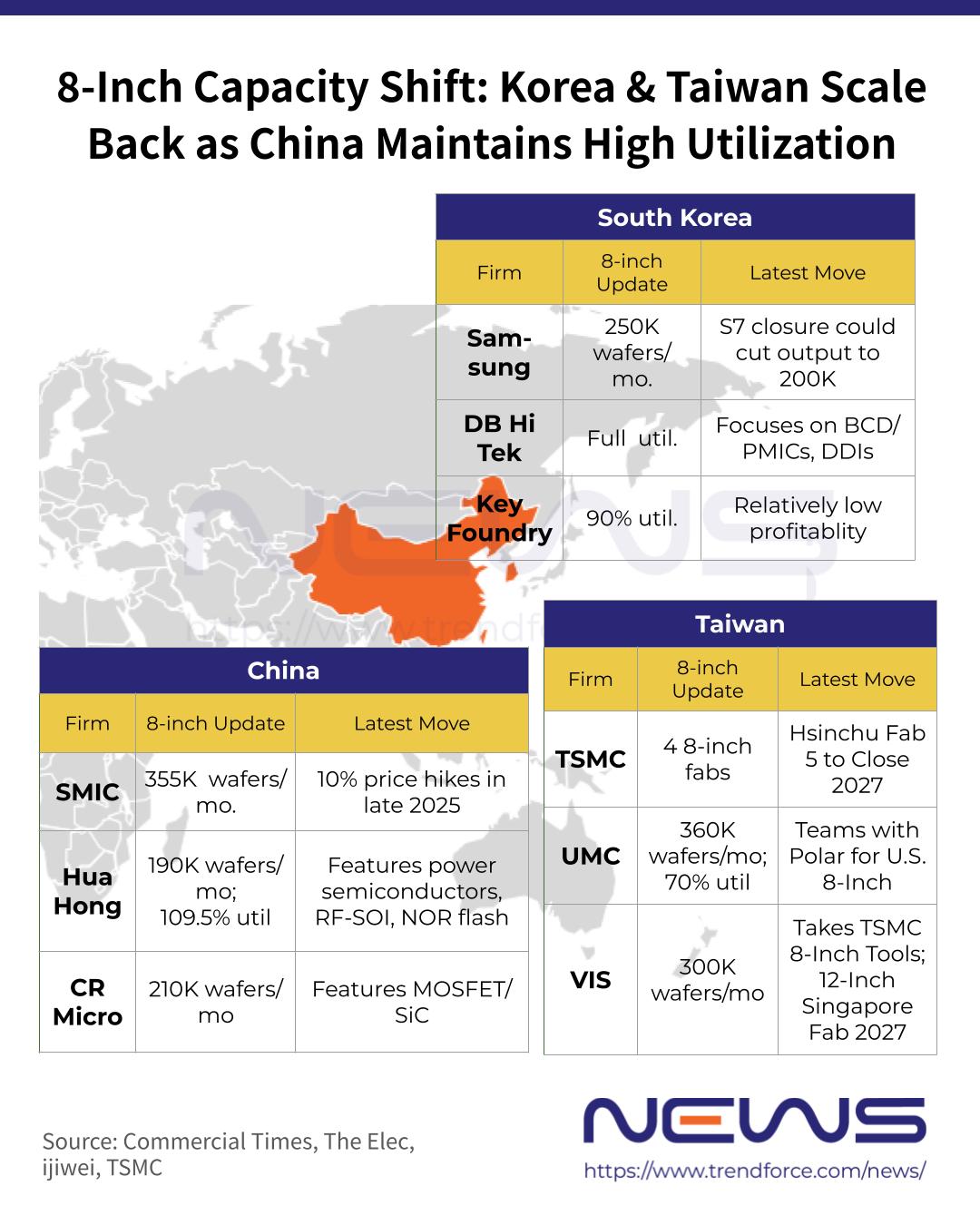
...TSMC, Samsung shift to advanced nodes; China's SMIC, Hua Hong seize 8-inch demand
As top foundries pivot to cutting-edge chips, Chinese rivals move to capture legacy-node orders
Samsung, SK hynix cut NAND output to drive profits amid AI-fueled demand
Memory giants favor DRAM investments as AI-era NAND shortages lift prices across devices
broadsword
Brigadier
China races to build HBM gear ecosystem amid US curbs, targets HBM3 ramp
Local vendors rush to fill HBM tooling gaps as Beijing leans on homegrown etch and packagingBy
Published 2026.01.20
As China's memory semiconductor corporations, including CXMT, prepare to begin mass production of high bandwidth memory (HBM) this year, they are said to be tightening the reins to build a semiconductor equipment ecosystem needed for HBM manufacturing. With U.S. restrictions expected to be the biggest obstacle to securing advanced semiconductor equipment for China's HBM production, they appear to be going all-in on internalizing equipment.
According to the industry on the 20th, Chinese semiconductor equipment corporations Naura Technology, Maxwell and U-Precision are accelerating efforts to develop equipment specialized for HBM from tools previously used in DRAM manufacturing. Because HBM is produced by stacking multiple DRAMs, advanced processes different from conventional commodity DRAM fabrication—such as etching to create channels for stacking semiconductors and packaging to bind them into a single chip—are applied, requiring equipment optimized for these steps. China's memory semiconductor industry is also shifting away from investment centered on commodity DRAM to focus its capabilities on dedicated processes and facility expansion for HBM production.
As China embarks on massive investment to secure leadership in the artificial intelligence (AI) industry, HBM is essential to run advanced AI Semiconductor chips. However, with HBM designated as a restricted item under U.S. advanced semiconductor industry controls, supply has faced difficulties. Currently, only three corporations—Samsung Electronics, SK hynix and Micron—mass-produce and supply HBM. In China, some say the HBM supply crunch is hampering growth in the AI industry.
Not only CXMT but also YMTC, the No. 1 NAND flash corporation in China, has jumped into HBM development. CXMT plans to mass-produce fourth-generation HBM (HBM3) this year and is assessed to have the technology to supply samples to domestic AI Semiconductor corporations such as Huawei. YMTC is said to have begun developing Through Silicon Via (TSV) used in HBM. TSV is a technology that drills microscopic holes in the chip to connect the top and bottom chips with electrodes and stack them to achieve high capacity and high bandwidth.
With U.S. restrictions expected to make it difficult to procure semiconductor equipment for HBM mass production, China's semiconductor equipment industry has begun work to build its own ecosystem. In particular, China is said to be focusing on processes such as etching and packaging needed in semiconductor manufacturing. Etching to precisely drill consolidation channels between DRAM chips for stacking, and packaging based on that to make a single chip, are known to have the greatest impact on HBM process Production yield.
A semiconductor industry official said, "Chinese semiconductor equipment corporations have internalized a considerable portion of DRAM process equipment, excluding extreme ultraviolet (EUV) lithography tools that draw ultra-fine circuits," adding, "However, for making HBM from commodity DRAM, areas such as etching and packaging still require technological reinforcement."
To that end, corporations such as Naura Technology, Maxwell and U-Precision are rolling out HBM-specialized equipment one after another. Naura Technology, the No. 1 corporation with more than a 30% share of China's etching equipment market, said it has built a portfolio of core process tools needed for HBM manufacturing, including not only etching equipment but also deposition to lay thin films on wafer surfaces and cleaning equipment. Maxwell has developed next-generation hybrid bonding equipment that bundles multiple DRAMs, and U-Precision said it has the equipment needed for HBM packaging.
Alibaba's AI chip company, Pingtouge Semiconductor, plans to IPO.
Alibaba Group is preparing to take its in-house AI chip subsidiary, Pingtouge Semiconductor (also known as T-Head), public, according to sources familiar with the matter. The move follows surging investor interest in Chinese AI chipmakers aiming to challenge Nvidia’s dominance in the AI accelerator market.
As a first step, Alibaba plans to restructure Pingtouge into a partially employee-owned entity before exploring an initial public offering (IPO)—though no timeline or valuation has been confirmed. Established in September 2018, Pingtouge is a wholly owned Alibaba unit with a full-stack portfolio spanning cloud and edge AI chips, including data center and IoT processors, covering the entire chip design chain.
The IPO bid underscores Alibaba’s strategic push to secure critical hardware for its cloud and AI ambitions. With CEO Wu Yongming committing over $53 billion to AI and infrastructure—and signaling even higher future investments—Alibaba is positioning itself as a global AI leader, akin to OpenAI. The recent full upgrade of its Qwen AI app in November 2025 further signals its push into consumer-facing AI services.
The planned IPO comes amid China’s intensified AI chip race, ignited by breakthroughs like DeepSeek, with Alibaba emerging as one of the most aggressive investors in the sector.
Chipsea Technologies' BMS chip CBM9680 has obtained ASIL-B functional safety certification.
On January 21, Chipsea Technologies announced that its CBM9680 Battery Management System (BMS) chip designed specifically for 12V lithium-ion starter battery systems in automobiles—has successfully obtained ISO 26262 ASIL-B functional safety certification from DEKRA, a leading international inspection and certification body. This milestone validates the chip’s high reliability and safety, positioning it as a critical enabler for the automotive industry’s transition from traditional lead-acid to lithium-ion starter batteries.

The certification ceremony was attended by senior executives from both Chipsea Technologies and DEKRA, including DEKRA China’s Functional Safety General Manager Li Mingxun, who presented the certificate to XinHai’s Vice President Wan Wei. XinHai’s leadership in automotive and industrial IC development also participated, underscoring the company’s strategic commitment to automotive electronics.
Chipsea Technologies, a leading Chinese full-signal-chain IC designer, has already achieved ISO 26262 ASIL-D process certification from TÜV Rheinland and offers a growing portfolio of automotive-grade products. The CBM9680 joins other certified chips already mass-produced in smart cockpits, fast charging, and body control systems across major automakers.
The CBM9680 is engineered to meet the demanding requirements of modern 12V automotive systems, which now support not only engine starting but also advanced electronics like ADAS and infotainment. Lithium-ion batteries offer superior energy density, longer lifespan, and faster charge/discharge cycles compared to lead-acid batteries—but require highly sophisticated BMS solutions to ensure safety and performance under extreme conditions.
Key Features of CBM9680:
- High-Precision Monitoring: Integrated high-accuracy ADCs measure voltage, current, and temperature with millivolt and percentage-level precision. Multi-channel VADC and differential Coulomb counting enable accurate state-of-charge tracking. Built-in and external NTC sensors monitor cell and ambient temperatures to prevent thermal runaway.
- Comprehensive Protection: Real-time hardware-based protections include overcurrent, overvoltage, under voltage, short-circuit, and thermal protection—with microsecond-level response. Additional features include cell disconnect detection, MOSFET impedance monitoring, and PACK+/PACK- short-circuit detection.
- Automotive-Grade Reliability: Certified to both ISO 26262 ASIL-B and AEC-Q100 standards, ensuring robust performance across extreme temperatures, vibration, and electrical noise throughout the vehicle’s lifecycle.
- Flexible Communication: Supports I²C (up to 1 MHz) and SPI (up to 4 MHz) interfaces for seamless integration with vehicle ECUs and intelligent management systems.