Chinese semiconductor thread II

tokenanalyst

Brigadier
Registered Member

The first hybrid silicon carbide product in China has been mass-produced​


Recently, Xpeng Motors and Xinlian Integrated Circuit jointly announced that China's first hybrid silicon carbide product has entered mass production, opening up a new path for improving the performance and reducing the cost of new energy vehicles.

This hybrid silicon carbide product was designed and developed by Xpeng Motors and jointly developed and put into mass production by Xinlian Integration. In this hybrid silicon carbide project, Xinlian Integration was responsible for the development and manufacturing of the power chip, as well as the development, implementation, and production of the packaging process. At "Xpeng AI Technology Day," Xpeng Motors announced that it will incorporate hybrid silicon carbide solutions into its future super electric and pure electric vehicles.

The hybrid silicon carbide technology introduced in this mass production initiative innovatively combines silicon and silicon carbide. A representative from Xinlian Integrated told China Electronics News that the biggest advantage of the hybrid silicon carbide solution over pure silicon carbide chip solutions lies in cost control. The high cost of silicon carbide material and the complex manufacturing process contribute to the high cost of pure silicon carbide chips. The hybrid solution reduces the amount of silicon carbide used.
Please, Log in or Register to view URLs content!
 

tokenanalyst

Brigadier
Registered Member

Yuntian Semiconductor's glass-based IPD technology: Leading breakthroughs in size and performance of high-frequency passive devices​


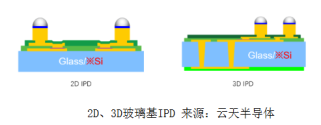
As demand for high-end applications such as 5G/6G communications , millimeter-wave radar (above 24GHz), and AI computing chips continues to rise, integrated passive device (IPD) technology is becoming a key link in supporting the development of these fields. IPD technology is widely used in core passive components such as filters, duplexers, power splitters, attenuators, and couplers. Improving device performance is inseparable from the support of high-quality substrate materials. Compared to traditional silicon substrates, glass substrates, with their excellent properties such as low dielectric loss, high thermal stability, high resistivity, and adjustable thermal expansion coefficient, provide an ideal platform for achieving higher performance and higher integration of passive devices, and also lay the material foundation for related technological breakthroughs.​

1756238625363.png

As a leading company deeply engaged in the field of through-glass via (TGV) technology, Yuntian Semiconductor has relied on its continuous deep cultivation and innovative breakthroughs in this field, focusing on the iterative upgrade of TGV and related processes, and successfully developed and launched glass-based IPD devices covering a wide range of application scenarios. It provides core passive solutions for cutting-edge applications such as 5G/6G communications, millimeter-wave radar, and high-speed interconnection, filling many technological gaps in the domestic high-end passive device field.

Yuntian Semiconductor and Xiamen University have recently collaborated to develop millimeter-wave passive components, achieving excellent test results and overcoming multiple design and process limitations. 24 passive components of varying structures and sizes, including transmission lines, filters, and resonant rings, were successfully integrated onto an 8-inch glass wafer. These components, based on their unique structural designs, demonstrate differentiated and superior performance, operating across a frequency range of 5 GHz to 90 GHz. They not only meet the needs of applications in the sub-6 GHz band, but are also adaptable to millimeter-wave and even higher frequency bands, providing flexible and efficient options for diverse applications.

the final test results and simulation data for this product are essentially consistent, fully validating the reliability and stability of the technology. In terms of performance, it demonstrates excellent transmission performance with low insertion loss, precise filtering characteristics, and remarkable high selectivity.​


Please, Log in or Register to view URLs content!
 

tokenanalyst

Brigadier
Registered Member

Guoke Testing completed tens of millions of yuan in A+ round financing, and is a third-generation semiconductor and new energy testing equipment manufacturer.​


Suzhou Guoke Testing Technology Co., Ltd. ("Guoke Testing") recently completed tens of millions of yuan in Series A+ financing, exclusively invested by Jinan High-Tech Science and Technology Investment Group. The funds raised will primarily be used to expand production lines for third-generation semiconductor and new energy test equipment, advance R&D of wafer-level inspection equipment, and mass-deliver high-end flying probe testers. They will also be used to accelerate the company's global strategic expansion. This marks another significant step forward in the capital market for the company, following its Series A financing in October 2024.

1756240540305.png
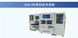
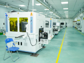
Public information shows that Guoke Testing was established in August 2019 and focuses on the research and development and industrialization of testing equipment in the third-generation semiconductor and new energy fields. It is the only company in China that can test packaging substrates, wafers, high-end flexible boards and camera modules. The flying probe testers and AOI automatic optical inspection equipment it developed have achieved domestic substitution, solving the "bottleneck" technical problems in related fields, and have been maturely applied in large quantities by leading companies in the industry and military industrial groups. In 2023, Guoke Testing established a wholly-owned subsidiary in Dongguan, Guangdong, and entered the new energy field. It mainly develops and produces capacity aging detection equipment and machine vision inspection equipment required for the production of new energy batteries.

Please, Log in or Register to view URLs content!

Please, Log in or Register to view URLs content!
 

tphuang

General
Staff member
Super Moderator
VIP Professional
Registered Member

AI端侧概念股持续走强,瑞芯微,乐鑫科技双双创历史新高 8月27日早盘,AI端侧概念股集体拉升,SoC芯片板块领涨。截至目前,乐鑫科技股价上涨逾16%至218元,而瑞芯微强势涨停,两者双双创下历史新高。 从业界来看,AI端侧应用加速落地,产业链热度持续升温。多家国际科技巨头近期动作颇多,其中,Meta计划在下月举行的Meta Connect大会上正式发布Hypernova智能眼镜,进一步推动端侧AI生态发展。 截至发稿,瑞芯微股价报215.6元,涨幅10%。
Looks like Rockchip and Espressif have both hit all time high in market cap. AI edge devices, SoC for boards have both seen huge demand coming up. Both are the de facto market leaders in what they do
 

Alb

Junior Member
Registered Member
One fabrication plant dedicated to producing Huawei’s AI processors is scheduled to start production as soon as the end of this year, while two more are due to launch next year, said two people with knowledge of the plans.
While the new plants are designed to specifically support Huawei, it is not clear who exactly owns them. Huawei denied having plans to launch its own fabs and did not provide further details.
Combined capacity from these three new plants, once fully ramped up, could exceed the current total output of similar lines at Semiconductor Manufacturing International Corporation (SMIC), China’s leading fab, according to those people with knowledge of the effort.
The people added that SMIC also planned to double its capacity next year for making chips at 7 nanometres — the most advanced mass-produced type in China. Huawei is SMIC’s largest customer at present for such processor lines.

Please, Log in or Register to view URLs content!
 

tphuang

General
Staff member
Super Moderator
VIP Professional
Registered Member

I put together a thread on this article. Very interesting and frankly not surprising since we anticipated all along (based on hvpc comment and satellite photos and bid info) that the jump in SMSC capacity & production is coming between 2025 & 2026. Huawei also said that all the obstacles will be resolved this year. So, the entire tech war initiated by Eric Schmidt and Biden admin was on very flawed logic.
 

tokenanalyst

Brigadier
Registered Member

Weijian Intelligent completed over 100 million yuan in Series B financing and is a domestic high-end packaging equipment manufacturer​

Weijian Intelligent Packaging Technology (Shenzhen) Co., Ltd. (Weijian Intelligent) recently completed a Series B financing round exceeding 100 million yuan. Investors include Qianhai Financial Holdings, Mingshi Capital, Lihe Science and Technology Innovation, Haitong Capital, and Share Investment. The funds raised from this round will be primarily used for product research and development, focusing on strengthening R&D and product development in the future of advanced packaging for transmission, storage, and computing in the AI era.

According to public information, Weijian Intelligence was established in 2019 and focuses on the research and development and production of high-precision and complex process chip packaging equipment. Its main products are the MV full range of high-precision die bonding equipment, which supports the packaging process requirements of third-generation semiconductor chips (gallium nitride, silicon carbide). It is a key equipment for core chip packaging in the fields of optical communications, 5G RF, commercial lasers, high-power IGBT devices, storage, etc.

Die bonding is the first critical step in chip packaging, and its accuracy directly determines the final product performance. Weijian Intelligent specializes in high-precision chip packaging equipment. Its core die bonding machine achieves 1.5μm accuracy, offering high stability and repeatability, breaking the monopoly of overseas manufacturers in the high-end market.

1756305838212.png

In July 2025, the expansion of Weijian Intelligent's Phase III delivery center was completed, increasing annual production capacity to 600 units. The delivery cycle for standard equipment was shortened by over 20%, generally within 1-3 months, effectively alleviating the current pressure on order delivery. The Phase IV production line is also under active development.

The Phase III production and delivery center at MicroVision Intelligence has further improved process accuracy to 0.5μm (e.g., the MV-05A product). This not only fills a technological gap in domestic high-end packaging equipment, but also, through capacity expansion, meets the exploding demand for high-precision equipment in optical communications, 5G RF, LiDAR, and other fields.

Please, Log in or Register to view URLs content!
 

tokenanalyst

Brigadier
Registered Member

Sanan Optoelectronics' 8-inch wafer project is officially launched!​


Sanan Optoelectronics recently revealed on its investor interaction platform that its Hunan Sanan 8-inch silicon carbide chip production line has been put into operation. This also means that Hunan Sanan Semiconductor has officially transformed into an 8-inch SiC vertically integrated manufacturer.
San'an Optoelectronics said that currently, Hunan San'an has a 6-inch silicon carbide supporting production capacity of 16,000 pieces/month, an 8-inch silicon carbide substrate production capacity of 1,000 pieces/month, and an epitaxial production capacity of 2,000 pieces/month. The 8-inch silicon carbide chip production line has been put into operation. It also has a silicon-based gallium nitride production capacity of 2,000 pieces/month.
In addition, Anyifa has put the production line into operation in February 2025, with an initial construction capacity of 2,000 pieces/month; Chongqing Sanan has initially built a production capacity of 2,000 pieces/month and has begun to gradually release production capacity.
The Hunan Sanan SiC project, with a total investment of 16 billion yuan, aims to create a vertically integrated mass production platform for 6-inch and 8-inch SiC wafers, encompassing the entire industry chain. Upon reaching full production, the project will have an annual production capacity of 360,000 6-inch SiC wafers and 480,000 8-inch SiC wafers.

Please, Log in or Register to view URLs content!
 
Top