Wait, 5nm next year? What lithography machines is Huawei using?
I put together a thread on this article. Very interesting and frankly not surprising since we anticipated all along (based on hvpc comment and satellite photos and bid info) that the jump in SMSC capacity & production is coming between 2025 & 2026. Huawei also said that all the obstacles will be resolved this year. So, the entire tech war initiated by Eric Schmidt and Biden admin was on very flawed logic.
You are using an out of date browser. It may not display this or other websites correctly.
You should upgrade or use an alternative browser.
You should upgrade or use an alternative browser.
Chinese semiconductor thread II
- Thread starter vincent
- Start date
Tungsten-doped amorphous carbon deposited by plasma enhanced chemical vapor deposition for dry etching hardmask applications
Yangtze Memory Technologies Co., Ltd
Abstract
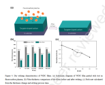
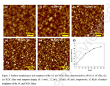
The dry etching hardmask with excellent physical and chemical properties is an urgent need for high-aspect-ratio etching process in semiconductor devices. Amorphous carbon is one of the significant interests for improving silicon based dielectric layer etching performance. In this study, tungsten doped amorphous carbon films were fabricated by plasma enhanced chemical vapor deposition (PECVD). X-ray photoelectron spectroscopy (XPS), atomic force microscopy (AFM), X-ray reflectometry (XRR) and nanoindentation were used to evaluate the film characteristics of the tungsten doped amorphous carbon. The results showed that film roughness, mass density, hardness and modulus were highly related to tungsten content, indicating that amorphous carbon film properties could be tuned by heterogeneous element doping. Dry etching tests show that increased tungsten content results to lower etch rate during long-time etching process. High-resolution transmission electron microscopy (HRTEM) and selected-area electron diffraction (SAED) indicated that tungsten carbide nanocrystalline regions were formed in higher tungsten doping films, which contributes to the etch resistance to fluorocarbon plasma.
Cambricon's revenue in the first half of the year increased by 43.48 times year-on-year to 2.88 billion yuan.
Cambricon released its performance report for the first half of 2025. The report showed that the company achieved revenue of 2.88 billion yuan in the first half of the year, a 43.48-fold year-on-year increase. The revenue growth was mainly due to the company's continued market expansion and active support for the implementation of artificial intelligence applications during the reporting period. Revenue in the reporting period increased significantly compared with the same period last year.
The substantial growth in operating income drove Cambrian's net profit attributable to shareholders of the parent company to RMB 1.038 billion in the first half of the year, turning losses into profits year-on-year; the non-net profit was RMB 913 million, turning losses into profits year-on-year.
Among them, Q2 achieved revenue of 1.769 billion yuan, a month-on-month increase of 59.19%; net profit attributable to shareholders of the parent was 683 million yuan, a month-on-month increase of 92.03%.
As of the end of June, Cambricon's total assets were 8.42 billion yuan, a year-on-year increase of 25.34%; the net assets attributable to shareholders of the listed company were 6.755 billion yuan, a year-on-year increase of 24.58%. The net cash flow from operating activities also turned from negative to positive to 911 million yuan.
Hunan University: Constructing SiC layer on diamond surface, breaking through the heat dissipation bottleneck of composite materials.
As electronic devices continue to evolve toward miniaturization and higher power, heat dissipation issues for chips and power modules are becoming increasingly prominent. Highly thermally conductive packaging materials have become a key bottleneck in the electronics industry. Among the many candidate materials, diamond/aluminum (Al) composites have attracted significant attention due to their low density, high thermal conductivity, and adjustable thermal expansion coefficient . However, these materials are prone to forming Al₄C₃ phases at the interface , which not only reduces stability but also hydrolyzes in humid environments, leading to rapid performance degradation.
To solve the above problems, the Hunan University team proposed a new method:
- First , a uniform silicon (Si) preset layer is deposited on the surface of diamond particles using magnetron sputtering ;
- Then, through vacuum annealing, Si is gradually converted into silicon carbide (SiC) ;
- Finally, it is combined with the aluminum matrix through pressure infiltration to form a stable composite material.
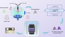
This strategy avoids direct contact between diamond and aluminum, effectively suppresses the large-scale generation of Al₄C₃, and at the same time improves phonon matching through the SiC layer, significantly improving the interfacial thermal conductivity .
The research team systematically examined the phase transitions of the silicon pre-layer at different annealing temperatures and found that its evolution sequence was amorphous Si, crystalline Si, and the coexistence of Si and SiC, ultimately transforming completely into a uniform and dense SiC layer at 1300°C. This SiC coating, approximately 400 nanometers thick, bonded firmly to the diamond, preventing cracking or flaking even at high temperatures. Accordingly, the interface structure gradually shifted from the traditional "diamond-Al₄C₃-aluminum" to "diamond-SiC-a small amount of dispersed Al₄C₃-aluminum," forming a more stable channel that facilitates heat conduction.
The optimized interface significantly improves the thermal conductivity of the composite material. Experimental results show a maximum thermal conductivity of 723 W·m⁻¹·K⁻¹, surpassing that achieved with conventional preparation methods. Furthermore, because the SiC coating effectively inhibits the formation of Al₄C₃, this composite material exhibits improved stability in hot and humid environments, avoiding performance degradation due to hydrolysis.
Lianghuo Rapid Annealing Furnace: Excellent Performance Leads to a New Benchmark in the Industry
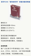
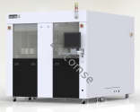
In the semiconductor manufacturing process, rapid thermal annealing (RTA) and rapid thermal processing (RTP) play critical roles. The performance of rapid annealing equipment directly impacts production efficiency and product quality. Lianghuo Semiconductor Equipment (Shanghai) Co., Ltd. has introduced its Lianghuo Rapid Annealing Furnace, which stands out among competitors with exceptional performance characteristics.
Exceptional Heating and Cooling Speeds
The Lianghuo rapid annealing furnace excels in heating speed. The S801 model can rapidly heat wafers to the required high temperature up to 1300°C—with a maximum heating rate of 150°C/second, significantly outperforming conventional RTA equipment. This fast ramp-up enables higher throughput in time-sensitive production environments. For example, during IC wafer fabrication, rapid heating quickly activates dopant atoms, reducing process time and boosting overall yield.
Cooling performance is equally impressive: the furnace can cool from 1000°C to 300°C at a rate of up to 200°C per minute, ensuring fast and stable temperature reduction. This precise cooling prevents thermal stress in semiconductor materials—especially crucial for compound semiconductors such as GaAs, SiC, and GaN. By minimizing internal stresses and defects, it enhances material integrity and improves product yield. Many other furnaces suffer from temperature fluctuations during cooldown, compromising quality.
Cooling performance is equally impressive: the furnace can cool from 1000°C to 300°C at a rate of up to 200°C per minute, ensuring fast and stable temperature reduction. This precise cooling prevents thermal stress in semiconductor materials—especially crucial for compound semiconductors such as GaAs, SiC, and GaN. By minimizing internal stresses and defects, it enhances material integrity and improves product yield. Many other furnaces suffer from temperature fluctuations during cooldown, compromising quality.
Superior Temperature Accuracy and Uniformity
Lianghuo’s furnace features a patented multi-zone real-time synchronized PID temperature control system, achieving an accuracy of just ±0.1°C. This high-precision control ensures that wafer temperatures remain tightly regulated throughout the annealing process, which is essential in critical processes like ion implantation annealing. Accurate thermal management guarantees consistent dopant activation and diffusion—directly impacting electrical performance consistency across devices.
For temperature uniformity, Lianghuo employs a dual-side heating configuration, significantly reducing pattern loading effects (a common issue in single-sided heating). This results in excellent thermal uniformity—≤0.5% of the set temperature—especially important for large-diameter wafers such as 12-inch wafers. Poor thermal uniformity can lead to uneven processing, causing over- or under-annealing in different regions. Quanhuo’s advanced design ensures consistent treatment across the entire wafer surface, improving product quality and reliability.
For temperature uniformity, Lianghuo employs a dual-side heating configuration, significantly reducing pattern loading effects (a common issue in single-sided heating). This results in excellent thermal uniformity—≤0.5% of the set temperature—especially important for large-diameter wafers such as 12-inch wafers. Poor thermal uniformity can lead to uneven processing, causing over- or under-annealing in different regions. Quanhuo’s advanced design ensures consistent treatment across the entire wafer surface, improving product quality and reliability.
Flexible Multi-Gas Configuration and Customizable Vacuum System
The S801 furnace supports a multi-gas configuration (customizable for additional gas lines), allowing precise control over gas flow rates and ratios tailored to specific process requirements. For example, in certain semiconductor processes requiring controlled nitrogen or oxygen environments, this flexibility enables accurate reaction conditions and greater process adaptability.
Equipped with a vacuum chamber featuring pressure stabilization, the furnace achieves high vacuum levels using molecular pumps—allowing users to customize vacuum degrees according to their needs. In high-purity applications such as high-temperature annealing where oxidation must be avoided, this high-vacuum capability ensures minimal contamination and maintains process purity. Unlike some competing furnaces that lack sufficient gas control or adjustable vacuum performance, Quanhuo’s solution meets the stringent demands of advanced semiconductor manufacturing.
Equipped with a vacuum chamber featuring pressure stabilization, the furnace achieves high vacuum levels using molecular pumps—allowing users to customize vacuum degrees according to their needs. In high-purity applications such as high-temperature annealing where oxidation must be avoided, this high-vacuum capability ensures minimal contamination and maintains process purity. Unlike some competing furnaces that lack sufficient gas control or adjustable vacuum performance, Quanhuo’s solution meets the stringent demands of advanced semiconductor manufacturing.
So I haven't been following the news regarding China's semiconductor situation that well, and I was just wondering if someone could give me an overview of where China currently is with EUV and DUV processes?
Earlier in the year, there was rumours that an EUV machine was being trialled and images of an LDP tool being tested at the Huawei Dongguan facility. I haven't heard anything from that since.
There was also news about a breakthrough in solid-state EUV lighting, however again, I haven't heard any developments from that.
Is there anyone out there with better information that can get me up to date with China's EUV projects? I've also heard things about how CIOMP (Chinese Institute of Optics, Mechanics and Physics) are the leaders for China's EUV development, whilst other organisations like Tsinghua University are assisting.
There isn't much coverage of what's going on, but I think western news outlets don't have the greatest insight into Chinese academic and scientific developments. Maybe here is a better place for that sort of information.
Thanks for your time!
Requirements for the precision environment required by lithography machines.
A photolithography machine is a core piece of equipment in semiconductor manufacturing. Its function is to precisely transfer the integrated circuit pattern on a mask onto a photoresist-coated wafer surface through optical projection, completing the graphical transfer process of the circuit pattern. In the chip manufacturing process, photolithography is the most complex and costly step, accounting for one-third of the total wafer manufacturing cost and 40%-60% of the manufacturing time, directly determining the chip's process accuracy and production yield.
The core principle is to use a high-energy laser as a light source. After the beam passes through the mask, it is reduced to a 1/16 scale by a focusing lens system. It is then precisely focused on the wafer surface, causing the photoresist to react with light, thereby completing the high-precision replication of the circuit pattern. This is equivalent to carving a city map on a strand of hair. The complexity and technical challenges are imaginable, and the operating environment is extremely demanding.
These precision requirements are mainly reflected in the following aspects:
1. Temperature stability:
The optical components (such as lenses and mirrors) and precision mechanical structures within photolithography machines are often made of extremely temperature-sensitive materials. Slight temperature fluctuations can cause the materials to expand and contract, leading to focal shift in the optical system, misalignment in the alignment system, and position drift in the mechanical stage. Ultimately, this can lead to pattern distortion, increased overlay error, and a sharp drop in yield. The entire photolithography area is typically maintained under constant temperature control.
2. Humidity stability:
Excessively high humidity can cause condensation on optical lenses, rust metal components, and alter photoresist properties. Excessively low humidity can easily generate static electricity, attracting dust and contaminating wafers and equipment. Precise humidity control is crucial to ensuring process stability and material performance.
3. Ultra-low vibration:
Lithography machines require extremely high stability during exposure. Any vibration from the ground (traffic, construction, personnel movement), the equipment itself (air conditioning, pumps), or the building (wind load) will directly cause jitter in the optical system, blurring or shifting the image projected onto the silicon wafer. Therefore, lithography machines are typically installed deep underground on independent foundations or high-performance active or passive isolation platforms, and some even employ technologies such as magnetic levitation for active vibration reduction.
4. Ultra-clean environment:
A speck of dust larger than the exposed pattern features lands on the mask or wafer and can block light, causing pattern defects or short circuits. At the nanoscale, even the smallest particles can be deadly. The entire lithography area is housed in a top-tier cleanroom, where air undergoes multiple stages of high-efficiency filtration, and strict purification procedures are in place for both personnel and materials entering and exiting.
5. Airflow stability:
Stable laminar flow can effectively and smoothly remove particles and heat generated during the process, prevent particles from settling on the wafer surface, and maintain temperature uniformity within the area. Turbulent airflow will swirl particles and may cause temperature fluctuations.
6. Anti-static and electromagnetic shielding:
Static electricity can attract dust, contaminating wafers and equipment, and even damaging sensitive microelectronic structures. The sophisticated sensors, control systems, and measurement systems (such as laser interferometers) within lithography machines are highly susceptible to interference from external electromagnetic fields, leading to inaccurate measurements or control errors.
Jicce (Nanjing) focuses on precision environmental control solutions and currently serves many global leading semiconductor, communication equipment, display panel companies and national key laboratories, and is used in many scientific research and production scenarios.
Currently, our high-precision environmental control equipment has achieved a maximum temperature control accuracy of ±0.002°C and a cleanliness level of Class 10 or higher. Our comprehensive, customized capabilities cater to diverse user environments and requirements, including temperature and humidity stability, cleanliness, vibration resistance, magnetic shielding, and sound insulation , ensuring we remain at the forefront of ultra-high-precision environmental control technology innovation.
High-speed parallel two-photon laser direct writing technology.
Two-photon laser direct writing is an emerging micro-nanofabrication technique. This technology utilizes a femtosecond laser to induce two-photon polymerization of photoresist at the laser's focal point, enabling feature sizes up to hundreds of nanometers. Combined with a piezoelectric stage or laser scanning device, it enables the high-precision fabrication of arbitrary three-dimensional structures. Currently, this technology has been widely applied in a variety of key fields, including micro-nano optics, materials, life sciences, microfluidics, micromechanics, and integrated optics.
Multi-beam parallel writing technology can effectively increase writing speed and is an important path for the further advancement and development of two-photon laser direct writing technology. It is expected to achieve high-speed processing of high-precision, large-scale structures. However, current parallel writing technology still has many problems in terms of generation methods, writing strategies, and splicing accuracy, which require continuous improvement and refinement.
Innovative work
To effectively increase the speed of two-photon laser direct writing, a team from the Center for Intelligent Chips and Devices at Zhijiang Laboratory designed and demonstrated a rotating mirror-based multi-beam parallel writing system. As shown in Figure 1, this system utilizes a spatial light modulator (SLM) to generate multiple beams, which are then independently modulated by a multi-channel acousto-optic modulator (AOMC). Furthermore, a polygonal rotating mirror replaces the traditional galvanometer, combined with a high-speed air bearing stage and a piezoelectric stage to achieve high-speed 3D scanning.
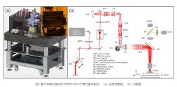
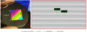
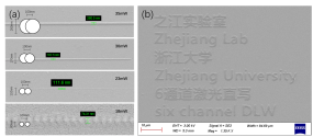
After testing, the system achieved a single-channel scanning speed of 7.77 m/s and can perform simultaneous parallel writing on up to six channels, with an equivalent maximum speed of 46.62 m/s. Figure 2(a) shows the characteristic dimensions of the system. As can be seen, as the laser power decreases from 35 mW to 18 mW, the line width decreases from 260 nm to 80 nm; however, after 150 nm, the pattern begins to transform from lines to a dot matrix. This is because at high rotation speeds, the direct writing speed of the objective lens focal plane approaches 8 m/s. At this time, the interval between two adjacent pulses is approximately 100 nm, making it impossible to effectively fill the gap and form a dot matrix. Therefore, the characteristic dimension of this system is approximately 150 nm. Using a higher repetition rate laser or reducing the pulse interval at a lower rotation speed can achieve smaller characteristic dimensions.
I suspect this is bogus information. Those 3 fabs are likely the 100,000 wpm SMIC 28 nm fabs at Shanghai, Beijing, and Tianjin. But those are unable to make leading edge chips.One fabrication plant dedicated to producing Huawei’s AI processors is scheduled to start production as soon as the end of this year, while two more are due to launch next year, said two people with knowledge of the plans.
While the new plants are designed to specifically support Huawei, it is not clear who exactly owns them. Huawei denied having plans to launch its own fabs and did not provide further details.
Combined capacity from these three new plants, once fully ramped up, could exceed the current total output of similar lines at Semiconductor Manufacturing International Corporation (SMIC), China’s leading fab, according to those people with knowledge of the effort.
Only SMIC SMSC can make FinFET chips and that should have 70,000 wpm capacity with the recent expansion.
China has also had imports of the best immersion lithography tools banned. So the expansion likely used already imported tools.
Unless Chinese industry magically delivered the immersion lithography tools but I am less than hopeful.
Last edited:

