Chinese semiconductor thread II

tokenanalyst

Brigadier
Registered Member
Orders are expected to increase by 300%, and the construction of the second phase of wafer line will be promoted

On February 8 , Longteng Semiconductor issued a statement saying that the company 's power semiconductor orders will increase threefold this year, and the construction of the second phase of the 8-inch production line is being accelerated.

In an interview, Chen Qiaoliang, executive president of Longteng Semiconductor, said that the company is making every effort to accelerate the construction of the second phase wafer production line for the 8- inch power semiconductor device manufacturing project, which will fill the gap in this field in Shaanxi Province.

Longteng Semiconductor will continue to deepen its transformation and upgrading, comprehensively covering the research and development, design, materials, wafer manufacturing, IGBT module packaging lines, as well as market expansion and application promotion of power semiconductors, aiming to achieve deep integration and coordinated development of the entire industry chain.

In terms of orders, during the Spring Festival, Longteng Semiconductor's production lines maintained 24- hour uninterrupted operation to fully meet market demand. Qiu Songjie, general manager of the company's manufacturing division, said that the production tasks in the first quarter have been close to saturation, and orders are currently scheduled for six months later. It is expected to increase by more than 2 times year-on-year, and the annual year-on-year growth is expected to reach more than 300% .

Please, Log in or Register to view URLs content!
 

tokenanalyst

Brigadier
Registered Member

SPPE-GAN: A novel model for Die-to-Database alignment and SEM distortion correction framework​

Abstract​

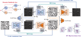
In the inspection stage of semiconductor manufacturing processes, hotspots detection is a critical task for enhancing yield. Die-to-Database (D2DB) technology allows for the comparison of actual chip images from electron beam inspection (EBI) with design databases, enabling quick identification of potential hotspots. However, D2DB faces challenges with imprecise localization on high-density chips, frequently necessitating intricate manual corrections that diminish detection efficiency. Additionally, scanning electron microscope (SEM) images can suffer from field distortion, compromising detection accuracy. To address these challenges, we propose an unsupervised SEM pattern extraction model (SPPE-GAN). This model adeptly integrates local, global, and keypoint information to precisely identify pattern locations within SEM images, subsequently transforming them into graphic data system (GDS) style images. Building on SPPE-GAN, we employ scale-invariant feature transform (SIFT) detection and the fast library for approximate nearest neighbors (FLANN) algorithm for precise matching between SEM images and their corresponding design layouts. After matching, optical flow methods are applied to indirectly correct inherent distortions in SEM images. In experiments on industrial datasets, our framework achieved over a 10% improvement in contour intersection over union (IoU) compared to assessments by experienced engineers. Moreover, under the same matching algorithm conditions, the SPPE-GAN outperformed widely used supervised methods like pix2pix and current state-of-the-art unsupervised style transfer techniques.

1739373281486.png

Please, Log in or Register to view URLs content!
 

supercat

Colonel
Top Chinese chip designer goes back to Tsinghua University to teach the next generation specialists.

Top chip designer Sun Nan leaves US and finds ‘room to play’ in China​

Tsinghua University highlights professor who has returned to China to train next generation of chip experts and tackle tech problems

Tsinghua University chip expert Sun Nan's return to China went largely unnoticed in the wave of Chinese scientists returning from abroad - that is, until last week, when the prestigious university in Beijing put a social media spotlight on the professor who has helped create more than 50 cutting-edge chips in a little over four years.
Please, Log in or Register to view URLs content!
 

tokenanalyst

Brigadier
Registered Member
Never let a good crisis go to waste.​

Manufacturing should be self-reliant, Saimet firmly empowers domestic substitution​


On the evening of the 2nd, the Bureau of Industry and Security (BIS) of the U.S. Department of Commerce issued an "enhanced version" of new export control regulations, adding 136 Chinese entities and 4 overseas subsidiaries of Chinese entities to the Entity List. More semiconductor products such as semiconductor equipment and high-bandwidth memory chips were included in export controls, and core software tools were also blocked.
In the current environment, there is no absolute safety since the first ban. However, misfortune often brings good fortune. The domestic substitution of semiconductors is accelerating, and the more bans are imposed, the stronger they become. A group of excellent companies are building a solid backbone for China's semiconductors.

1 Upgrade again and face challenges together

The sanctions directly target semiconductor equipment manufacturing, materials, memory chip HBM, Fab factories, and even EDA software tools and some investment institutions are included. For the semiconductor industry, any obstruction in any link will affect the progress of the entire industry. The US hopes to restrict or delay the development of my country's semiconductor industry in the form of "patching". However, by 2024, my country's semiconductor manufacturing industry has grown its own wings, strong local companies are accelerating breakthroughs, and domestic substitution is gradually getting better. "The overall impact is controllable and will not have a substantial impact on the company's operations." Many companies involved in the ban have issued similar statements. The sword of Damocles is hanging over our heads, but we also have our own plan B. Among the companies involved in the ban are customers served by Symet, who took early warnings, established firewalls early, and unswervingly chose domestically developed systems to protect the core of the factory, effectively reducing the risk.

As a leading semiconductor CIM company, Saimet is the only domestic manufacturer with mass production cases in the field of 12-inch semiconductor [silicon wafer production, wafer manufacturing, packaging and testing]. The fully automated CIM solution developed by Saimet can provide dozens of software products such as MES, EAP, SPC, YMS, APS, RTD, etc., to help semiconductor factories realize production process automation, ensure efficient allocation of resources, and provide strong data support for production decisions.
As domestic substitution reaches a critical moment, a group of "pure-blooded" companies like Saimet have emerged, joining hands with the semiconductor industry to meet challenges and jointly shoulder the mission of independent control of technology and localization of the supply chain.

2. Accumulate strength and then develop, and intelligent manufacturing should be self-reliant

The security of the semiconductor supply chain has become the core of the international game. Sanctions are both a crisis and an opportunity.
Nowadays, my country's semiconductor industry is gradually breaking through the bottleneck of high-end technology. Through continuous R&D investment and technology accumulation, related companies have gradually made certain breakthroughs in independent and controllable technology. Especially in the fields of storage, communication chips and intelligent manufacturing, a complete industrial chain has been gradually established.
Since its establishment, Saimet has been committed to independent and self-reliance around semiconductor intelligent manufacturing, creating the PlantU series of products to support factories in building intelligent manufacturing systems with high availability, high efficiency, stability, scalability and flexibility. Through a variety of analysis, reporting and KPI functions, it analyzes massive data, monitors anomalies, predicts and analyzes, helping to maximize production and operation efficiency, ensure the stability of production quality, and lay a solid foundation for the development of my country's semiconductors.

SinoMet has worked with customers to successfully implement a number of benchmark projects. Specifically:
● Build a fully automated CIM platform for a 6-inch fab to boost both production and yield
● Replaced the MES system for an 8-inch plant, recasting the efficient production line and protecting the core engine
Achieve efficient and high-quality fully automated production for 12-inch factories in SH, HB, CD and other locations
From MES, EAP to SPC, YMS, APS and other systems,
Sinomet provides targeted system services to many customers, protecting the development of semiconductor companies from all directions and angles. Semiconductors have always been engraved in Sinomet's genes. We firmly embrace the needs of industrial upgrading and help every customer cross the critical stage of domestic substitution.


Please, Log in or Register to view URLs content!
 

tokenanalyst

Brigadier
Registered Member

The impact of aberrations in extreme ultraviolet lithography systems on exposure results​


Abstract
Extreme ultraviolet (EUV) lithography is one of the essential technologies for the 5nm and below technology nodes. However, the presence of aberrations in the system severely affects the exposure results, which can lead to wafer rework and increase costs. In order to investigate the impact of aberrations in EUV lithography systems on exposure results, this paper conducts research on the impact of aberrations on exposure results of patterns that commonly used in EUV single-exposure for the 5nm technology node. A large number of aberration experiments are performed, and the distribution of critical dimension (CD), normalized image log-slope (NILS), Pattern Shift (PS), and process variation band (PVB) of exposure results in relation to all Zernike terms variation within ±50mλ is statistically analyzed. We find that aberrations lead to worse exposure results generally, and the distribution of results does not strictly follow a Gaussian distribution but exhibits significant "tail" phenomena. And the impact of aberrations varies for different patterns. Furthermore, the relationship between the distribution of exposure results and the magnitude of aberrations are investigated. It is observed that as the aberration RMS increases, the probability of deteriorated exposure results also increases. Spherical aberration has a significant impact on CD and PVB, while x-direction coma has a significant impact on the PS of vertical line-space patterns, and y-direction coma has a significant impact on the PS of vertical tip to tip patterns. X-direction astigmatism has a higher probability of causing positive PS, while y-direction astigmatism has a higher probability of causing negative PS. Relatively speaking, the effects of 3-foil, 4-foil, and 5-foil aberrations are smaller. This paper provides a clear reference for the influence of various aberrations on exposure results and can contribute to the future development and aberration control of lithography systems.​

Please, Log in or Register to view URLs content!
 

tokenanalyst

Brigadier
Registered Member

Highly Effective Broadband Extreme Ultraviolet Light Source by Spatially Confined Plasma.​

Abstract​

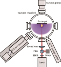
Broadband extreme ultraviolet (EUV) radiation has shown significant advantages in advanced-node semiconductor metrology. To meet the high-volume manufacturing demands of advanced nodes, the conversion efficiency of a laser-plasma broadband EUV source was studied. First, the wavelength and spectral intensity of the EUV spectrometer were calibrated and used to characterize the total conversion efficiency (CE) from laser to EUV radiation at 10-20 nm. Subsequently, an in-situ second pulse was applied to a solid Sn target using a 1 μm laser, thereby achieving a broadband EUV conversion efficiency of 52.5% in the 10-20 nm range, which is the highest CE reported so far. The main reason for this is that the curved surface formed by the ablation of the first laser pulse caused spatial constraints on the tin plasma. These spatial constraints were induced by the subsequent laser pulse and resulted in a significant increase in EUV emission. This study provides a new approach for generating a broadband EUV light source with high CE, presenting a novel method of semiconductor microchip metrology for advanced technology nodes of the future.​
1739384495705.png

Conclusion​


With the reduction of feature size and the emergence of more complex three-dimensional structures in advanced nodes, higher requirements are put forward for measurement in the semiconductor manufacturing process, and the measurement methods based on EUV broadband light sources have gradually shown great advantages. In view of the development demand of desktop EUV broadband light sources for advanced node semiconductor measurement, this paper carried out optimization research on the broadband radiation of 10~20 nm band of laser-generated tin plasma. The second pulse bombardment was carried out on the solid Sn target after the first pulse by 1 μm laser, and the conversion efficiency of 10~20 nm EUV broadband radiation of tin plasma was characterized by a self-developed EUV spectrometer. The in-situ second pulse achieved a conversion efficiency of up to 52.5%, which is the highest conversion efficiency reported in the extreme ultraviolet band so far. This is because the groove formed by laser ablation can effectively confine the tin plasma generated by the second pulse, and the EUV luminescence time is prolonged and the emission area is increased, which effectively increases the emission of plasma. In addition, with the increase of laser energy, the optical thickness of tin plasma gradually increases, especially the optical thickness of tin plasma constrained by grooves is significantly improved, which leads to the increase of radiation self-absorption of tin plasma near 13.5 nm. This competitive relationship between emission and absorption ultimately increases the total luminous efficiency of tin plasma in the 10-20 nm radiation range. The above research results provide new ideas for the development of high-conversion-efficiency EUV broadband light sources for high-throughput semiconductor measurement.

Please, Log in or Register to view URLs content!
 

tokenanalyst

Brigadier
Registered Member

Chongqing releases new policy to focus on the development of high-end chips and devices​


The Chongqing Integrated Circuit Design Industry Development Action Plan (2023-2027) proposes that by 2027, the city's integrated circuit design industry revenue will exceed 12 billion yuan, with more than 100 new companies, including more than one company with revenue exceeding 500 million yuan and more than four companies with revenue exceeding 200 million yuan. The focus will be on the design of analog chips, silicon photonic chips, automotive chips, power semiconductors, MEMS sensors and other design fields, and promote the design level to be the leading in the country.

For the packaging and testing industry, the Chongqing Integrated Circuit Packaging and Testing Industry Development Action Plan (2023-2027) proposes that by 2027, the city's integrated circuit packaging and testing industry revenue will exceed 20 billion yuan, with more than 10 new companies, including more than 2 companies with revenue exceeding 500 million yuan. The focus will be on developing packaging and testing technologies for compound semiconductors, power semiconductors, silicon photonic chips, and MEMS sensors.

In the manufacturing process, Chongqing plans to introduce foundry lines with mature process nodes, and plans to build foundry plants with mature process technology of 28-55nm, attracting leading foundry companies to set up in Chongqing. In addition, Chongqing is also promoting the construction of 12-inch integrated circuit feature process lines, focusing on the development of automotive-grade chips.

In general, Chongqing has formed a full chain of "chip design - wafer manufacturing - packaging and testing - raw material matching". Key enterprises such as China Resources Microelectronics, SK Hynix, and China Electronics Technology Group Corporation are concentrated in Chongqing. In addition, as one of the world's largest notebook production bases, Chongqing has a huge production capacity of smart terminals and complete vehicles, which provides a huge market space for the development of the chip industry. Especially in the automotive industry, automotive-grade chips have become an important part of the "chain filling" of Chongqing's automotive industry chain.

Please, Log in or Register to view URLs content!
 

tphuang

General
Staff member
Super Moderator
VIP Professional
Registered Member
alright, I did the very hard work of listening to SMIC earnings call, so you all don't have to

Please, Log in or Register to view URLs content!

here is my summary. I think the message around reshuffling of supply chain to domestic suppliers is pretty clear.
China region accounted for 85% of SMIC revenue, increased by 34% YoY
Due to reshuffling in supply chain & increase in customer market share as part of domestic supply drive
12-inch wafer accounted for 77%, increased 35% YoY, due to increase in capacity
Analog BCD, DDIC, CIS platform continue to grow
Analog continued to improve in high voltage, high performance area in 8 & 12 inch tech platforms
In High voltage DDIC, SMIC continue to deliver 28nm high VC Mode max into production
Ultra lower power consumption and performance enhancement
In CIS & ISP, offered higher resolution, smaller pixel size & higher density
rapidly introduce image processing solution with better performance & ultra lower power consumption.
Newly launched power discrete platform with mass production for smart phones & industrial control
Continue to introduce high performance and high reliability product for high voltage, lower power consumption platforms
All received auto grade certification, looking to cover more parts of EVs like infotainment system & power train.
Auto supply chain is reshuffling toward domestic suppliers, some product started production.
SMIC receiving a lot of orders from consumer, connectivity & phones, a lot of rush orders for first half of the year.
ASP went up by a little bit in Q4, because it’s normally a light season, but the lower utilization meant higher 12-inch ratio, so ASP is higher
For Q1 & Q2, they got so much rush order that even their 8-inch capacity is full.
ASP will come down a little bit, because 8-inch ratio is up due to the rush orders. Utilization continue to go up
Need to add more product & platform to have higher ASP.
Capex & capacity increase will be about the same as 2024 in 2025. Capacity increase is based on long term contracts established already.
Goal is to continue to grow steadily, regardless of good or bad years. Goal is to add 50k wpm of 12-inch wafers per year, no more 8-inch growth
In terms of equipment, can’t always control when equipment will arrive. 2023 added $7.5B and 2024 added $7.33B.
Expect to be able to get equipment on time this year (this like indicates domestic supply chain is getting close to solid by this point, no major worries from sanctions)
Would like to grow to getting 1/3 of the orders from the China’s auto market.
In Q4, auto sector accounted for 8 to 10% of SMIC’s revenue. Goal is for revenue to grow to 10% of overall revenue.
Goal is to make all the platforms auto grade.
Depreciation will affect company’s margins in 2025.
SMIC is growing a lot in 2025H1 vs last year due to the stimulus policies from Chinese government in consumer electronics sales. (Nobody else can see it)
SMIC is the only one that can fully benefit from China’s consumer growth and domestic supply chain reshuffling.
 

tokenanalyst

Brigadier
Registered Member
YMTC breakthrough is forcing Samsung to upgrade their NAND production in China to stay competitive which is pretty much a lost for the stooges in D.C.

Samsung's Xi'an plant will upgrade to 286-layer NAND flash memory process.​


Samsung Electronics is upgrading its Xi'an, China plant to a 286-layer (V9) NAND flash memory process to cope with the current market downturn and fend off growing competition from Chinese semiconductor companies.

Samsung has been pushing to transition its mainstream 128-layer (V6) NAND process to a 236-layer (V8) production line at its Xi'an plant since 2023. However, the company decided to go a step further and install a V9 production line. Samsung plans to introduce new equipment required for the process in the first half of this year and plans to build a production line with a monthly capacity of 2,000 to 5,000 wafers in the second half of the year.

The transformation is part of Samsung's broader strategy to maintain its technological leadership and ensure long-term product competitiveness.

The Xi'an plant is Samsung's only overseas memory production base and is critical to the company's global supply chain, accounting for about 40% of its total NAND production. The upgrade to the 286-layer NAND process is expected to significantly increase the plant's production capacity.

1739395765585.png

 
Top