You are using an out of date browser. It may not display this or other websites correctly.
You should upgrade or use an alternative browser.
You should upgrade or use an alternative browser.
Chinese semiconductor thread II
- Thread starter vincent
- Start date
1 billion yuan semiconductor headquarters project settled in the West Coast
1 billion yuan semiconductor headquarters project settled in the West Coast
The semiconductor equipment R&D and production headquarters project with a total investment of 1 billion yuan by Haichuang Intelligent Equipment (Yantai) Co., Ltd. settled in Qingdao West Coast New Area.
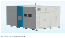
This project is the second high-end semiconductor equipment project to be implemented in the New District this year. The project will select a location in the New District to build a semiconductor equipment R&D and production headquarters, develop and manufacture wafer-level permanent bonding, temporary bonding, debonding equipment and other products, and plans to combine domestic industry needs and its own technological advantages to develop into a well-known domestic semiconductor equipment company.
It is reported that Haichuang Intelligent Equipment (Yantai) Co., Ltd. was established in 2017. It has layout in international and domestic markets and is committed to the research and development, manufacturing and sales of high-end semiconductor equipment. It has more than 60 related patents.
The new generation of information technology industry is one of the leading industries of Qingdao's "10+1" innovative industrial system. It is listed in a priority development position and leads the "10+1" key industrial direction. In the main track of new generation information technology, the integrated circuit industry is the top priority. The wafer-level bonding equipment and other products independently developed and produced by Haichuang Intelligent Equipment are of great significance to improving the localization rate of equipment of my country's semiconductor enterprises and breaking the international monopoly. The implementation of this project will further strengthen the integrated circuit industry chain of the new district, inject new vitality into the development of the city's high-end integrated circuit equipment industry, and help the industry move to new heights.
Electronic ceramics and silicon dioxide manufacturer ACEINNA Technology restarts IPO
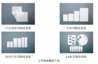
Electronic ceramic products: mainly focusing on alumina ceramic substrates, ceramic structural parts and electrostatic chucks The company's electronic ceramic products mainly include alumina ceramic substrates, ceramic structural parts and electrostatic chucks. Alumina ceramic substrates have the main advantages of high temperature resistance, high electrical insulation performance, small dielectric constant, low dielectric loss, high thermal conductivity, good chemical stability, and thermal expansion coefficient close to that of components. The company's ceramic substrates are manufactured by the cast film method, which has the characteristics of high production efficiency, good surface finish of the produced film strips, and stable performance. The main applications are ceramic substrates for chip resistors, photovoltaics, electric vehicles, LEDs, etc.
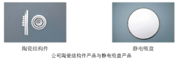
The electrostatic chuck is an ultra-clean wafer adsorption device suitable for use in a vacuum environment. It uses the principle of electrostatic adsorption to evenly clamp ultra-thin wafers. In integrated circuit manufacturing, it is a core component of high-end equipment such as etcher, chemical vapor deposition (CVD) equipment, physical vapor deposition (PVD) equipment, and ion implantation machines. The electrostatic chuck products developed by the company are designed and processed in accordance with relevant standards of the semiconductor industry. The performance indicators meet market demand and have passed the certification of downstream domestic semiconductor industry leaders such as Yangtze Memory, Silan Microelectronics, and North Huachuang and achieved sales.
12-inch silicon wafer final polishing equipment was approved
In order to meet the high quality requirements of IC chip circuit processes with line widths less than 0.13μm to 28nm for 300mm diameter silicon polished wafers, further reduce the contamination of impurities such as metal ions on the surface of the silicon wafer, and ensure that the surface of the silicon wafer has extremely high surface nano-morphology characteristics, final polishing (fine polishing) becomes an indispensable key step .
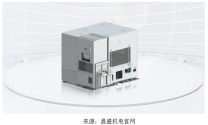
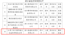
The 12-inch silicon wafer final polishing equipment selected by Changsheng Electromechanical this time has successfully broken through a number of key technologies such as flexible and uniform pressurization of the polishing head, effectively improved the uniformity of the wafer surface, fully guaranteed the stability and reliability of the product, and the overall technology has reached the international advanced level. While meeting the polishing needs of large-size single-crystal silicon wafers, it has achieved independent research and development and domestic substitution of key core components and consumables, providing strong technical support for the research and development of large-size silicon wafer manufacturing and equipment for high-end integrated circuits in China.
Predictable downstream effect of sanctions, and also an excellent opportunity to gain market share from TSMC.
No point spending 100 of billions if the capacity to use them isn't there. The government is doing what is needed by the industry. Spending more wouldn't change much.It's not alarmism, I know China is making progress. But compared to the kind of money US tech firms are throwing at AI vs what China's big fund is spending is a bit disappointing. Especially when you look at the media articles which constantly talk about how China is spending huge on semiconductors. But the actual numbers are really low compared to even one US big tech company. China's total GDP is now 20 trillion dollars. Considering the national importance of Chip self reliance, The national Chip spending should be several 100 billion compared to current big fund budget of just 48 billion.
Plus SMIC market is mostly just China and their capacity is limited. While TSMC is a global giant and the most advanced fab company in the world and they get contracts from companies around the world. In short the world is their market hence their size and revenue will always be bigger except something groundbreaking happens to change that. SMIC meanwhile is limited to Chinas market and they are also under sanctions with the type of equipment they can use. So they have to be much more prudent.
The first mass-produced printed OLED has been delivered to customers
The reporter learned from the Hubei Provincial Department of Science and Technology that the "Wuhan New Display Industry Innovation Joint Laboratory" of TCL Huaxing Wuhan Base has been established in the base's R&D building. After three months of trial operation, the laboratory produced its first results. The world's only mass-produced printed OLED 21.6-inch 4K professional display was officially delivered to customers in Wuhan.
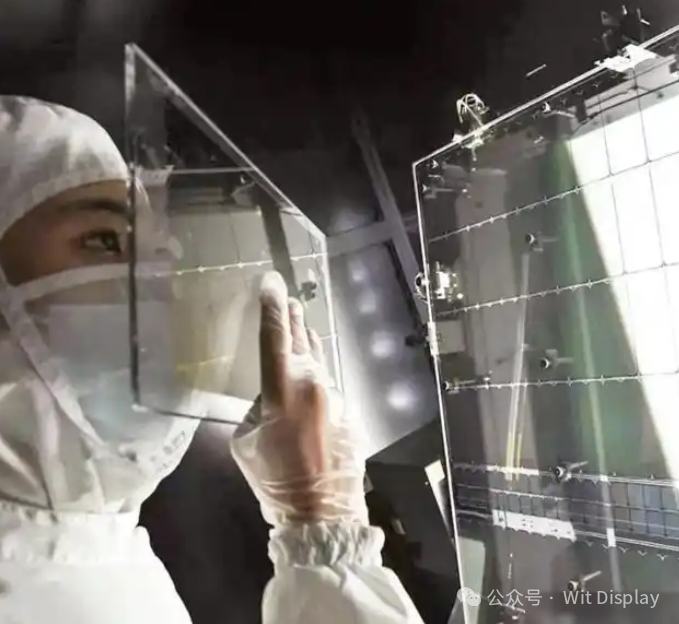
It is understood that printed OLED is the next-generation technology that TCL Huaxing focuses on, and it is also the first technology in the display industry that Chinese companies have led to enter the commercial stage globally. The relevant person in charge of the laboratory introduced that universities, enterprises and innovation platforms have worked together to create a highland for technological innovation, talent training and industrial chain collaboration in Optics Valley, further promoting the cluster-coordinated and high-quality development of the semiconductor display industry in Wuhan.
A "screen" brings multiple parties together, and then "rolls" outwards together, competing not on price but on innovation. The innovation of the new display industry must change the previous model of relying on a certain company to concentrate on breaking through technology and expanding scale, and strengthen the upstream and downstream collaboration of the industry in innovation. The laboratory adopts the "industry chain co-construction model" to connect the upstream and downstream, and jointly plan, build and share the industry chain. During the Spring Festival holiday, upstream material and manufacturing equipment suppliers, midstream module assemblers and downstream scenario application parties are working together to tackle key problems.
It is understood that the laboratory is led by Wuhan Huaxing Optoelectronics, a leading semiconductor display technology company, and jointly established with Jingli Electronics, Jingwei Technology, Huarui Optoelectronics, Huazhong University of Science and Technology, and Wuhan New Display Technology Achievement Transformation Pilot Platform. Focusing on future display devices and other directions, it will break through a number of key core technologies, bridge the gap from material research and development to application, and promote the development of domestic materials and key equipment driven by application needs, ultimately driving Wuhan's overall industrial scale to exceed 100 billion yuan, and the output value of small and medium-sized panels to become the world's first.
i remember, CXMT was the weakest link in Chinese semiconductor industry just 2 years ago.. look at now
According to media reports, CXMT is accelerating the development of next-generation DRAM technology. Instead of using 17nm as originally planned for the first commercial DDR5 product, it directly adopted 16nm process technology.
The next-generation 15nm process technology is also being developed based on the existing process, with the goal of developing the technology within 2025 and achieving commercialization as early as the second half of 2026.
Research firm TechInsights said that after CXMT completed the development of 17nm process technology, it immediately completed the development of 16nm process technology, so the first commercial DDR5 product used 16nm process technology.
CXMT is catching up quickly! 15nm will be developed this year and put into mass production next year
According to media reports, CXMT is accelerating the development of next-generation DRAM technology. Instead of using 17nm as originally planned for the first commercial DDR5 product, it directly adopted 16nm process technology.
The next-generation 15nm process technology is also being developed based on the existing process, with the goal of developing the technology within 2025 and achieving commercialization as early as the second half of 2026.
Research firm TechInsights said that after CXMT completed the development of 17nm process technology, it immediately completed the development of 16nm process technology, so the first commercial DDR5 product used 16nm process technology.
Automotive grade chips are introduced into OEMs, and half-bridge modules are supplied in batches
Xiyong Micro-Electronic Park announced on February 11 that China Resources Microelectronics held a new power module product launch conference, grandly launching a series of new products including various PIM modules, automotive main drive modules and IPM modules based on high-voltage super junction MOS , IGBT and SiC .
According to relevant persons in charge of China Resources Microelectronics, as of now, China Resources Microelectronics has achieved mass production of 56 automotive-grade power chips, which have officially entered the supply chain list of a certain OEM in Chongqing. Products represented by half-bridge power modules have been supplied in batches to many leading new energy vehicle companies in China.
The IGBT modules released by CR Micro in this new product launch are widely used in core components such as main drive inverters, on-board chargers (OBCs) and DC-DC converters. SiC modules include DCM series half-bridge power modules, MSOP series half-bridge power modules, and HPD series full-bridge power modules, which are mainly used in on-board chargers, main drive inverters and high-voltage DC converters of new energy vehicles. In addition, CR Micro also released dual-core MOS modules, which are used in body domain controllers of leading automotive customers. Currently, the cumulative shipments in the automotive field exceed 40 million.
China Resources Microelectronics' layout in Chongqing mainly includes a 12-inch power semiconductor wafer production line and an advanced power packaging and testing base, with a total investment of 11.75 billion yuan. The project aims to build a leading domestic automotive-grade semiconductor platform, covering the entire industrial chain of power semiconductors from wafer manufacturing to packaging and testing.
- 2-inch wafer production line: It will be officially put into operation in January 2023, with a planned monthly production capacity of 30,000 to 35,000 12-inch mid-to-high-end power semiconductor wafers, and equipped with 12-inch epitaxy and thin-film processes. Products cover medium and low voltage trench SGT MOS, high voltage super junction SJ MOS, etc., to meet automotive-grade requirements.
- Power Packaging and Testing Base: The first medium and low voltage SGT power device will roll off the production line in December 2023, with a yield rate of 99.5%. The project took only 360 days from start to completion, and the construction speed is leading in the industry. The base focuses on the automotive electronics and industrial control markets, providing module-level, wafer-level and other packaging and testing services.
By 2025, the Chongqing Park has become the core incremental practice site of China Resources Microelectronics. The utilization rates of its 8-inch and 12-inch production lines are maintained at above 90%, and the 12-inch production capacity ramp-up is progressing smoothly, laying the foundation for listing on the Science and Technology Innovation Board and market expansion.

