Chinese semiconductor thread II

tphuang

Lieutenant General
Staff member
Super Moderator
VIP Professional
Registered Member

Hangzhou Gallium Semiconductor applied for a patent for a method of slicing a polished gallium oxide single crystal substrate to reduce defects such as wafer cleavage, chipping and microcracks around the cutting path.​

According to information from the State Intellectual Property Office, Hangzhou Gallen Semiconductor Co., Ltd. has applied for a patent titled "A Slicing Protection Layer Structure for a Gallium Oxide Single Crystal Substrate Polishing Wafer and Its Slicing Method".
Information from the National Intellectual Property Administration shows that Hangzhou Gallen Semiconductor Co., Ltd. has applied for a patent titled "A slicing protection layer structure for a gallium oxide single crystal substrate polishing wafer and its slicing method", publication number CN 118752386 A, and application date August 2024.

The patent abstract shows that the present invention provides a slicing protection layer structure and slicing method for a gallium oxide single crystal substrate polishing wafer, which belongs to the technical field of processing gallium oxide single crystal substrate polishing wafers. The slicing protection layer structure of the present invention includes a stacked slope fixture, a carrier, a second soft protective layer, a gallium oxide wafer, a first soft protective layer and a hard protective layer from bottom to top, and the slope fixture ensures that the cutting path along the (010) crystal plane direction of the gallium oxide wafer is cut at a slope angle. In the present invention, the role of the first soft protective layer and the second soft protective layer is to prevent the surface of the polished wafer from being scratched by hard objects and contaminated by the cooling medium, and the role of the hard protective layer is to offset part of the normal force of the grinding wheel on the (100) easy cleavage crystal plane during the slicing process; the slope fixture will further decompose the normal force applied by the grinding wheel to the (100) crystal plane, thereby reducing the generation of defects such as wafer cleavage, collapse and microcracks around the cutting path. The dicing method of the present invention has a fast cutting speed and can directly dicing a polished wafer without causing defects such as scratches and contamination on the wafer surface.
View attachment 137571

Please, Log in or Register to view URLs content!

Please, Log in or Register to view URLs content!

Garen is pretty good. A month ago, they developed ultra thin Gallium Oxide 6-inch substrate, which solves the problem of low thermal conductivity for Gallium Oxide. There will be plenty of good application in power semiconductor

From a few months ago
Please, Log in or Register to view URLs content!
Compared with traditional Silicon Carbide semiconductor materials, the fourth-generation semiconductor material
Please, Log in or Register to view URLs content!
has a higher withstand voltage, lower cost, and higher energy saving efficiency. With its excellent performance and low-cost manufacturing,
Please, Log in or Register to view URLs content!
is mainly used to prepare power devices, radio frequency devices and detection devices. It is widely used in rail transit, smart grids, new energy vehicles, photovoltaic power generation, 5G mobile communications, national defense and military industries, etc. field.

In the next 10 years or so,
Please, Log in or Register to view URLs content!
devices are likely to become competitive power electronic devices and will directly compete with Silicon Carbide devices. In addition, the industry generally believes that in the future,
Please, Log in or Register to view URLs content!
is expected to replace
Please, Log in or Register to view URLs content!
and Gallium Nitride to become the representative of a new generation of semiconductor materials.
So these guys, Semicorex also got 6-inch Gallium Oxide industrialized and they say it can be used RF and military field. So, I'm looking forward to these appearing in radar or EW equipments.

Please, Log in or Register to view URLs content!
Fujia Gallium a month ago said they've started work for production line of 6-inch Gallium Oxide substrate line.

Looks like we are getting close to commercialization of Gallium Oxide
 

tphuang

Lieutenant General
Staff member
Super Moderator
VIP Professional
Registered Member
Isn't it Ga2O3?
Yes, I'm too lazy to spell out Ga2O3 every time.

It’s possible that they shifted to 3 nm if capacity opened up. But still need to see. We’ll probably have a good idea by spring of next year.
when the rumors came out, I think they said it was designed for N4 and aimed to achieve K9000S, so probably more for medium ranged phones, but we will see! not sure where they are getting the modem solution from
 

huemens

Junior Member
Registered Member
when the rumors came out, I think they said it was designed for N4 and aimed to achieve K9000S, so probably more for medium ranged phones, but we will see! not sure where they are getting the modem solution from
According to those rumors it's a collaboration with Unisoc and will use Unisoc modem.
 

tokenanalyst

Brigadier
Registered Member

Stress-Free Polishing: The Final TSV Optimization Step.​


Throughout this blog series, we've taken you on a journey through the various steps involved in developing and optimizing through-silicon vias (TSVs), which have become vital to packaging of many types of devices that require smaller-footprint, higher-density package stacks. Part 1 discussed TSV formation and the benefits of our SAPS™ megasonics for TSV cleaning; Part 2 explained electroplating and how our Ultra ECP system optimizes copper fill in the vias; and Part 3 examined the problem of TSV gaps and the solution that we've developed to mitigate this issue: our Ultra Pmax plasma-enhanced chemical vapor deposition (PECVD) solution . This last installment focuses on the final step: polishing. We will look at why the polishing step is so critical to TSV formation, how stress-free polishing is shaping the future of semiconductor manufacturing, and the market advantages brought by our Ultra Stress-Free Polishing solution.

Ultra SFP: Revolutionizing TSV polishing

We developed our Ultra Stress-Free Polishing (SFP) solution to meet the increasing demands of TSV manufacturing. This advanced technology offers several advantages over traditional CMP, making it particularly well-suited for TSV formation in high-performance and high-density semiconductor applications .

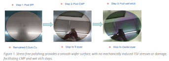
As the industry moves toward thinner wafers for improved performance and energy efficiency, Ultra SFP is specifically designed to handle these fragile substrates without introducing damage, unlike traditional CMP techniques. With its more refined polishing process, Ultra SFP greatly reduces the amount of mechanical force applied to the wafer, ensuring minimal stress. This is crucial in preventing common defects like TSV cracking, delamination, and wafer warpage. All of these defects affect planarity, which is key for ensuring that subsequent layers in the 3D IC stack align perfectly. Ultra SFP Provides superior control over surface uniformity, leading to excellent planarization across the entire wafer.

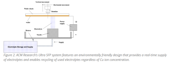
Another key advantage of Ultra SFP is its environmentally focused design (Figure 2). The tool has a built-in system for electrolyte recycling and reuse, enabling it to consume significantly fewer chemicals during processing. This enables semiconductor makers to improve their manufacturing sustainability for CMP and wet etch.​

1729548621170.png
1729548653276.png

Please, Log in or Register to view URLs content!
 

huemens

Junior Member
Registered Member

TechInsights: Huawei Mate XT Teardown​

Please, Log in or Register to view URLs content!
At the core of the Mate XT is the Kirin 980 processor, built on a 7nm process technology. This SoC includes an octa-core CPU (2.6 GHz Cortex-A76 and 1.92 GHz Cortex-A76) and a Mali-G76 GPU, enabling efficient multitasking and graphics rendering. The device is equipped with 8GB of LPDDR4X RAM and offers 512GB of UFS 2.1 storage, providing ample capacity for apps and media.
 

tokenanalyst

Brigadier
Registered Member

AIoT's multiple product lines have increased their market share, and Rockchip's net profit in the first three quarters increased by 354.9% year-on-year​

Rockchip released its third-quarter performance report, stating that from January to September, it achieved revenue of 2,159,606,597.14 yuan, a year-on-year increase of 48.47%; the net profit attributable to shareholders of the listed company was 351,709,019.93 yuan, an increase of 354.9% over the same period last year; the net profit attributable to shareholders of the listed company after deducting extraordinary gains and losses was 343,463,917.03 yuan, an increase of 417.142% over the same period last year.

Among them, the company achieved revenue of 911,004,357.3 yuan in the third quarter, a year-on-year increase of 51.36%; the net profit attributable to shareholders of the listed company was 168,936,946.15 yuan, an increase of 221.68% over the same period last year; the net profit attributable to shareholders of the listed company after deducting extraordinary gains and losses was 166,610,319.44 yuan, an increase of 224.03% over the same period last year.

Rockchip explained the reasons for the sharp increase in performance in the first three quarters as follows:
In the first three quarters of 2024, the demand for AIoT product lines showed a collective growth. The company leveraged the advantages of the "geese-shaped formation" layout of AIoT chips, with the RK3588 series as the flagship, to form a multi-level product combination punch that meets different needs in each product line, and leveraged the advantages of NPU in the implementation of AI algorithms to promote the continuous increase in the market share of multiple AIoT product lines.

At the same time, the company's new products such as RK3576, RK2118, and RV1103B were quickly introduced to leading customers in the target fields, creating new growth and will continue to release incremental value in the future.

Please, Log in or Register to view URLs content!
 
Top