Chinese semiconductor thread II

sunnymaxi

Captain
Registered Member
There is no direct competition between them in high-end nodes between TSMC and SMIC due to market access barriers. Its not like TSMC can sell its high-end nodes into China market, or SMIC can sell its high-end nodes in Western markets.

Huawei toppled Apple as #1 flagship China market share with **only** DUV 7nm, then even accessing a prototype EUV at 5nm will game-changing for Huawei. Absolutely game changing. Also, China is the world's largest semiconductor and mobile phone market, so the weight of a captive market favors SMIC, even without EUV yield parity or scale.
Why are we assuming there would be fair competition between SMIC - even a SMIC on the cutting edge - and TSMC in international markets? If we're talking about the mid-2030s timeframe when SMIC would be on the cutting edge of semiconductor manufacturing with enough volume to service the world market, we should also bear in mind that the balance of power vis-a-vis the US and China will be radically different than it is today.

We're talking about a China with ~1500 fifth gens, a 6th gen well into production, 50+ SSNs, H-20s, a complete strategic deterrent, etc. China can exert an enormous amount of pressure on Taiwan to accept restrictions on TSMC's activities, like "voluntary" production curbs a la Plaza Accords and sanctions on US companies that fab their chips at TSMC.
in December, 2020 Liang Mong said, we have completed 7nm R&D and by next year April, 2021 we will start risky production. we also carried out 8 different cutting edge techs include 5nm/3nm R&D and awaiting EUV machine to carry out final test.

in past 4 years, Chinese academy of science Microelectronics publish many research papers and Patents related GAA transistor and next generation CFET transistor.

Chinese Academy of Sciences' GAA transistor manufacturing process has made a breakthrough, helping nodes below 3nm
Please, Log in or Register to view URLs content!

its actually funny, Chinese institutes are doing all these research without having single prototype of EUV. this is what we called smart strategy. our preparation has completed now. we are just awaiting first EUV prototype to carry out physical test. all other Non-Litho tools entered in immersion stage 28nm/14nm include photoresists and EDA.

by 2030, the global face of semiconductor will be completely different. not what majority of people thinks now..
 

GulfLander

Junior Member
Registered Member

"Xiaomi Rumored to Have Taped out its First 3nm Chipset, Which Might be Launched Next Year​

Rumors have been circulating for a while that China’s tech giants are capable of manufacturing chips in advanced nodes even without the need for extreme ultraviolet (EUV) lithography machines by ASML, and that local foundry SMIC has reportedly produced 5nm chips for Huawei. Now there seems to be a new member joining the ranks of the elite. According to the reports by MyDrivers and Wccftech, Xiaomi has successfully taped out its first 3nm SoC.

Though more details are yet to be confirmed, Wccftech indicates that it is possible that Xiaomi will launch the 3nm chipset sometime next year.

Xiaomi, according to the reports, has been developing its own custom chipsets for years. The first product is believed to be Surge S1, which was released with the Mi 5c smartphone in 2017. The report by MyDrivers suggests that the Surge S1, built on 28nm node, is a 64-bit octa-core processor.

Following the Surge S1, Xiaomi went on to develop several chips, reportedly including the Surge C1, Surge G1, and Surge T1, according to MyDrivers.

The information of Xiaomi’s recent success in its 3nm chip tape-out is reportedly disclosed by Tang Jianguo, Chief Economist of Beijing Municipal Bureau of Economy and Information Technology, at Beijing Satellite TV, MyDrivers notes. Citing Tang’s remarks, Wccftech indicates that the achievement is described as a historic milestone for China.

Wccftech further notes that as companies like Huawei have been prohibited from doing business with TSMC or Samsung due to U.S. trade sanctions, if Xiaomi does have reached the tape-out stage for its 3nm chipset, it could enable other Chinese companies, including Huawei, to leverage this technology in their devices.

However, more details are yet to be confirmed, as there are no updates on whether the SoC will use TSMC’s N3E process or the more advanced N3P node, according to Wccftech. Additionally, details about the chipset’s CPU cluster, GPU, or whether it will feature ARM designs or a custom architecture remain unknown. Therefore, it would be better to approach this rumor with caution."

Please, Log in or Register to view URLs content!


measuredingabens

Junior Member
Registered Member
Provided the rumour is credible, the fact still remains that it isn't domestic fabs that will be fabbing the chips. SMIC and other Chinese foundries really need to expand advanced node capacity if they want to service more than just Huawei. Given the secrecy surrounding advanced node plans and the need to get EUV into service we probably won't get any wind of new fab plans until they've already started building. Even with the indicators that domestic equipment makers are advancing rapidly to <7nm nodes, it's going to be a while until we see more Chinese chip designers move to advanced nodes manufactured on the mainland.
 

tokenanalyst

Brigadier
Registered Member

Hangzhou Gallium Semiconductor applied for a patent for a method of slicing a polished gallium oxide single crystal substrate to reduce defects such as wafer cleavage, chipping and microcracks around the cutting path.​

According to information from the State Intellectual Property Office, Hangzhou Gallen Semiconductor Co., Ltd. has applied for a patent titled "A Slicing Protection Layer Structure for a Gallium Oxide Single Crystal Substrate Polishing Wafer and Its Slicing Method".
Information from the National Intellectual Property Administration shows that Hangzhou Gallen Semiconductor Co., Ltd. has applied for a patent titled "A slicing protection layer structure for a gallium oxide single crystal substrate polishing wafer and its slicing method", publication number CN 118752386 A, and application date August 2024.

The patent abstract shows that the present invention provides a slicing protection layer structure and slicing method for a gallium oxide single crystal substrate polishing wafer, which belongs to the technical field of processing gallium oxide single crystal substrate polishing wafers. The slicing protection layer structure of the present invention includes a stacked slope fixture, a carrier, a second soft protective layer, a gallium oxide wafer, a first soft protective layer and a hard protective layer from bottom to top, and the slope fixture ensures that the cutting path along the (010) crystal plane direction of the gallium oxide wafer is cut at a slope angle. In the present invention, the role of the first soft protective layer and the second soft protective layer is to prevent the surface of the polished wafer from being scratched by hard objects and contaminated by the cooling medium, and the role of the hard protective layer is to offset part of the normal force of the grinding wheel on the (100) easy cleavage crystal plane during the slicing process; the slope fixture will further decompose the normal force applied by the grinding wheel to the (100) crystal plane, thereby reducing the generation of defects such as wafer cleavage, collapse and microcracks around the cutting path. The dicing method of the present invention has a fast cutting speed and can directly dicing a polished wafer without causing defects such as scratches and contamination on the wafer surface.
1729521991799.png

Please, Log in or Register to view URLs content!


tokenanalyst

Brigadier
Registered Member

Yuanshan Semiconductor releases a new generation of high-voltage gallium nitride power devices​

Yuanshan Semiconductor recently released a new generation of high-voltage gallium nitride power devices and conducted detailed testing in Tektronix Advanced Semiconductor Laboratory

GaN power devices have become a popular choice in the market due to their high-speed switching capability, high power density and cost-effectiveness. However, due to the constraints of operating voltage and long-term reliability, the potential of these devices has not been fully realized and they mainly compete on price in the consumer electronics field. Recently, with the introduction of high-voltage GaN devices, we have seen their potential in a wider range of market applications.

Yuanshan Semiconductor recently released a new generation of high-voltage GaN power devices and conducted detailed tests at Tektronix Advanced Semiconductor Laboratory. These test results provide us with a comprehensive understanding of the performance of Yuanshan Semiconductor GaN power devices. At present, Yuanshan's existing products include sapphire-based GaN power devices of various specifications such as 700V, 1200V, 1700V, and 3300V. Many performance indicators are leading in the industry and are mainly used in high-power PD fast charging, car chargers, bidirectional DC-DC, micro inverters, portable energy storage, V2G and other fields.

1729522126135.png

Please, Log in or Register to view URLs content!
 

tokenanalyst

Brigadier
Registered Member

Shandong Youyan's silicon material project for etching equipment has been put into mass production​


It is reported that the total investment of the project is 357 million yuan, and it mainly produces large-size single-crystal silicon component processing products. After full production, 204 tons of silicon materials will be added annually. "Silicon material components for etching equipment mainly include silicon rings and silicon electrodes, which are core consumables required for the etching process of wafer manufacturing. They are mainly used to produce 8 to 12-inch plasma etchers, and play an important supporting role in etchers." Yan Zhirui, general manager of Shandong Youyan Ace Semiconductor Materials Co., Ltd., introduced.

Please, Log in or Register to view URLs content!
 

tokenanalyst

Brigadier
Registered Member

Ultra-precision intelligent shaping strategy for optical components using pulsed ion beams.​


Abstract:
With the ongoing advancement of optical systems, there has been a growing demand in recent years for precision optical components across various cutting-edge research fields, including EUV lithography lenses, synchrotron radiation X-ray mirrors, and strapdown inertial navigation laser gyro resonators. Ion Beam Polishing (IBP) technology is characterized by its ability to remove complex shapes with excellent stability, absence of edge effects, non-contact non-destructive processing, and high precision. It is commonly employed as the final finishing process for high-precision optical components. While there exist various optimization schemes for the current ion beam shaping machining paths and their velocity distributions, there are still instances where the machine tool's dynamic performance cannot meet the requirements of the optimized machining schemes when processing components with large gradient errors. We introduce a novel Pulsed Ion Beam (PIB) machining technique to overcome the limitations associated with current ion beams in the processing of high-precision optical components. This method not only offers ultra-high removal resolution but also significantly reduces the demands on machine tool dynamics , prevents the formation of extra removal layers, and adeptly achieves precise dwell times at each machining point on the component.

Results and Discussions The stability and linearity of PIB have been confirmed, with its removal resolution demonstrated to achieve material removal of 0.33 nm using just 5 pulses. The machining capabilities of traditional IBF and PIB in addressing gradient errors were compared through simulations. The results indicated that when the wavefront gradient of the surface shape error exceeds 0.5 λ /cm, the PIB offers a pronounced advantage in shaping. The implementation of the ant colony algorithm cut ineffective processing paths by 57% . Ultimately, the new processing strategy enabled the acquisition of surfaces with sub-nanometer precision. Following three stages of processing, the RMS error was reduced from 343.438 nm to 0.552 nm.

Conclusions This study introduces a new generation of ion beam processing techniques. Compared to traditional IBF methods, the PIB offers superior material removal resolution. By comparing the amounts of material removed with the same sputtering time but varying duty cycles, the PIB system's outstanding stability and linearity in material removal were confirmed. Additionally, five pulses were applied at a frequency of 1 Hz and a 10% duty cycle to sputter hafnium oxide thin films. The comparison of film thicknesses before and after processing confirmed that PIB achieves a sub-nanometer removal resolution of 0.066 nanometers per pulse. Simultaneously, the ACO algorithm was employed to optimize and plan the PIB machining paths, reducing ineffective paths by 57.7%. Ultimately, this processing strategy was used to fabricate an actual monocrystalline silicon mirror, achieving a sub-nanometer precision optical surface of 0.552 nm. This verifies the superior performance of the PIB processing strategy and system in achieving high-precision optical surfaces. It represents a more flexible, accurate, and efficient ion beam processing technique.​

1729525890107.png

Please, Log in or Register to view URLs content!
 

tokenanalyst

Brigadier
Registered Member

Oxidation of Silicon on Substrate Induced Bubble-Like Damage of Mo/Si Mirror Irradiated by Femtosecond Euv Pulses​

Abstract​

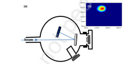
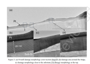
Mo/Si multilayers are commonly used as extreme ultraviolet (EUV) reflection coatings owing to their high reflectivity at EUV wavelengths. This study utilized Shanghai Soft X-ray Free-Electron Laser (SXFEL) to generate 13.5 nm, ~300 fs pulse lasers, and the laser damage behaviors of Mo/Si multilayers were investigated. The designed Mo/Si multilayer achieved high reflectivity at an incident angle of 20°. After exposing the surface to an average of 20 laser pulses per point at normal incidence, bubble-like damage was observed. Monte Carlo method was employed to obtain the energy absorption distribution of Mo/Si multilayers under EUV laser radiation. It was confirmed that the cause of EUV laser damage to Mo/Si multilayers was the enhancement of energy absorption, leading to the melting of the layers. High-energy absorption occurred at a place close to the substrate induced by the oxidation of Si and on the top of the multilayers, which resulted in multilayers detaching from the substrate and forming bubble-like morphology. This intensified interlayer diffusion and altered crystal orientation, resulting in irreversible damage to the multilayers.

1729526137647.png1729526182524.png


Please, Log in or Register to view URLs content!
 

tokenanalyst

Brigadier
Registered Member
YMTC improving 3D stacking with better PEALD precursors.​

Study on the damage mechanism and prevention technology of silicon dioxide on polysilicon by plasma enhanced atomic layer deposition.​

Yangtze Memory Technologies Co., Ltd

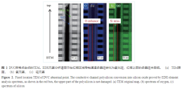
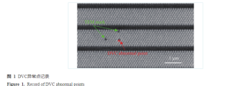
Abstract: The mechanism of irreversible damage to polysilicon caused by silylamide precursor byproducts during plasma enhanced atomic layer deposition (PEALD) of SiO2 was studied by electron beam inspection (EBI) . It is proposed to use monoamine silylamide as a precursor instead of polyamine silylamide to reduce the damage to polysilicon materials. Under the premise of not damaging polysilicon, the effect of monoamine precursor diisopropylamine silane (DIPAS) with less chemical steric hindrance on the reaction rate is further studied.

1729529587505.png1729529619074.png

Please, Log in or Register to view URLs content!
 
Top