Chinese semiconductor thread II

tokenanalyst

Brigadier
Registered Member

High-reliability silicon carbide chip packaging equipment supplier Zhongke Guangzhi completed A+ round of financing of tens of millions of yuan​


Zhongke Guangzhi recently completed its A+ round of financing, with a financing amount of tens of millions of RMB, invested by Chongqing Science and Technology Innovation Investment Group Co., Ltd. Chongqing Science and Technology Innovation Changjia Private Equity Investment Fund Partnership (Limited Partnership). Zhongke Guangzhi said that this round of financing will mainly be used to expand the semiconductor packaging equipment product line, support the deepening of silicon carbide chip packaging equipment R&D projects and the development of standardized packaging equipment products, strengthen the construction of the market sales system, and promote the company's layout in overseas markets.

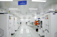
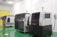
Founded in 2021, China Science and Technology Optoelectronics Co., Ltd. is a high-reliability semiconductor packaging equipment provider. It mainly provides industry customers with advanced process equipment and excellent solutions required for R&D and production in the domestic semiconductor, optoelectronics and advanced manufacturing markets. Based on the core team's many years of technical accumulation in the field of high-power semiconductor laser packaging and back-end packaging equipment, China Science and Technology Optoelectronics has independently developed a series of high-performance, high-quality, economical and practical packaging equipment products, mainly including plasma cleaning machines, vacuum eutectic reflow ovens, high-precision fully automatic placement machines, nano-silver pressure sintering machines and inert gas glove boxes. It covers the equipment requirements corresponding to the key process links of the back-end packaging of semiconductor chips, optimizes and guarantees the reliability and quality of packaging, and empowers multiple fields such as power semiconductors, optoelectronics, optical communications and laser packaging.

The headquarters of China Science and Technology Optoelectronics is located in Beibei Park, Western (Chongqing) Science City. It also has offices in Shenzhen, Xi'an, Beijing, Shanghai, Chengdu, Wuhan and other places, and conducts business in the domestic and international markets. Among them, the production base of the Chongqing headquarters covers an area of more than 10,000 square meters, with multiple product lines and public service platforms for semiconductor packaging test verification, and has good mass production and delivery capabilities. It has passed multiple ISO system certifications and has a process-based material control management system and a high-standard lean manufacturing production system.​

1729605864312.png1729605884908.png

Please, Log in or Register to view URLs content!
 

tokenanalyst

Brigadier
Registered Member

The "Shengmei (ACM Shanghai) Semiconductor Equipment R&D and Manufacturing Center" plant A was successfully capped​

The topping-out ceremony of Building A of the "Shengmei Semiconductor Equipment R&D and Manufacturing Center" was held in Lingang. Fu Xinhua, First-Class Inspector of Shanghai Municipal Commission of Economics and Information Technology, Xia Yuzhong, Deputy Director of Pudong New Area Science and Technology Commission, Lu Yu, Deputy Director of Lingang New Area High-Tech Department, Weng Kaining, Vice President of Shanghai Lingang Group, Chen Xiulin, Deputy Director of East China Branch of China Construction Third Engineering Bureau, Li Wenqiang, Chief Operating Officer of GalaxyCore Microelectronics, Pei Leihong, Director of Production Planning Department of Shanghai Huali, Xiang Yinan, Deputy General Manager of Shanghai Science and Technology Venture Capital (Group) Co., Ltd., Wang Hui, Chairman of Shengmei Semiconductor Equipment (Shanghai) Co., Ltd., Wang Jian, General Manager, as well as representatives of upstream and downstream enterprises in the industry chain such as suppliers, representatives of Shengmei shareholders and investors, representatives of Shanghai Integrated Circuit Industry Association, and representatives of project design units and general contractors attended the ceremony and witnessed this milestone moment.

The Shengmei Lingang project with a construction area of 138,000 square meters was officially capped. Currently, two R&D buildings, two high-rise factories, and one auxiliary factory are planned. At the same time, the auxiliary factory will be equipped with a R&D test clean room of the same level as the integrated circuit production line to accelerate the company's product process testing and verification and improvement and upgrade testing. In line with the goal of integrating R&D and production, Shengmei Shanghai has realized mixed R&D and production land in Lingang for the first time. After completion, the planned annual production capacity will exceed 600 units, with an annual output value of RMB 10 billion.

Wang Jian, general manager of Shengmei Shanghai, delivered a welcome speech. The "Shengmei Semiconductor Equipment R&D and Manufacturing Center" is Shengmei's first land acquisition project in Lingang, and it is an important milestone for Shengmei's development. Under the guidance of the "one body and two wings" spatial layout of Shanghai's integrated circuit industry, the project fully leverages the advantages of the "Zhangjiang-Lingang" dual-core development and north-south interaction to create Shengmei's major global R&D and production base, incorporate it into the overall layout of Shengmei's global development, and promote Shengmei to become a leading domestic comprehensive platform-type integrated circuit equipment group, rank among the first echelon of global integrated circuit equipment companies, and enhance the core competitiveness of China's integrated circuit equipment.

Please, Log in or Register to view URLs content!
 

tokenanalyst

Brigadier
Registered Member
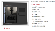
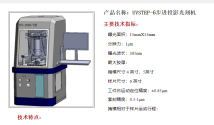
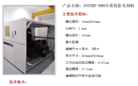
A bit of semiconductor history in China, there were other companies that tried to compete in the lithography market, at least in the IC/mems semiconductor market, but it seems they didn't succeed given the preference at the time for foreign systems and SMEE, but would have been an interesting competition for SMEE, forcing them to solidify their higher-end systems sooner.​

1729608890403.png1729609024572.png
1729608926410.png1729608978304.png

Please, Log in or Register to view URLs content!
 

tokenanalyst

Brigadier
Registered Member

A wafer fab in Shenzhen announced that the 8-inch SiC line will be put into production by the end of the year.​


Founder Microelectronics announced that as an IDM company in the field of third-generation semiconductors, the company currently has two fabs. Fab1 currently has a SiC production capacity of 9,000 pieces/month (6 inches), and is expected to reach 14,000 pieces/month by the end of 2024. In 2025, it will have an annual automotive-grade SiC MOS production capacity of 168,000 pieces, and the current GaN production capacity is 4,000 pieces/month. Fab2's 8-inch SiC production line will be put into operation at the end of 2024, with a long-term planned production capacity of 60,000 pieces/month. In addition, Founder Microelectronics' current automotive-grade SiC MOS production capacity ranks first in China.
1729612893145.png
Founder Microelectronics' series of products cover all scenarios of new energy vehicle applications: 1200V 16m/18m/20mΩ is used in main drive inverter controllers, 1200V 35m/60m/85mΩ is used in OBC, 1200V 60m/85mΩ is used in DC/DC, 1200V 60m/85mΩ is used in air conditioning compressors, 1200V 16m/20m/35m/60mΩ is used in charging piles and other scenarios. Founder Microelectronics' automotive-grade 1200V SiC MOS products have been used on a large scale, especially in the main drive controllers of new energy vehicles.

Please, Log in or Register to view URLs content!
 
Top