Jia Zhaowei of ACM Shanghai: Continuing to deepen the field of 3D chip integration
At the 13th Semiconductor Equipment, Core Components and Materials Exhibition (CSEAC 2025) on September 4, Jia Zhaowei, Vice President of Process at ACM Shanghai, delivered a keynote highlighting the company’s advancements in 3D chip integration. He emphasized that 3D stacking has become essential for boosting performance by integrating diverse functional chips, driving demand for advanced interconnect technologies like TSV and sub-micron interconnects, especially in HBM evolution from bumping to hybrid bonding.
Challenges include mechanical stress, warpage, coplanarity issues due to chip stacking, and difficulties in plating high-aspect-ratio vias and cleaning fine structures post-flip-chip assembly. In response, ACM Shanghai has developed a comprehensive portfolio of electroplating equipment leveraging proprietary innovations: the front-end Damascus system features a dual-anode design for uniformity and edge control, while advanced packaging tools use a second-anode technology to optimize electric field distribution and reduce plating deviation.
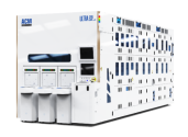
ACM’s solutions support 28nm and above processes across TSV, advanced packaging, and third-generation semiconductors. Beyond electroplating, the company has expanded into furnaces, PECVD, and Track systems, with R&D and manufacturing bases in Shanghai and South Korea, backed by a global service network.

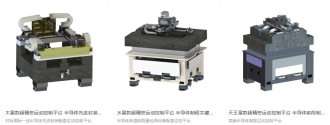
To meet panel-level processing needs, ACM introduced horizontal plating, edge etching, and negative-pressure flux cleaning equipment, patented solutions addressing wafer rotation control and process stability, many already in mass production.
Jia concluded that ACM is not only advancing localization but also solving industry pain points through original, differentiated technologies. The company remains committed to deepening innovation in 3D chip integration, driving technological progress, and capturing emerging market opportunities.


