Chinese semiconductor thread II

tokenanalyst

Brigadier
Registered Member

Canqin Technology's semiannual report reveals the company's latest news on ceramics​


Recently, Canqin Technology released its 2025 semi-annual report. The company's operating income, total profit, and net profit attributable to shareholders of listed companies increased by 52.76%, 56.41% and 51.94% respectively.

During the reporting period, the company not only continued to invest in mobile communications, radar and radio frequency circuits, satellite communications, navigation and positioning, aerospace and national defense science and technology, consolidated its leading position in existing businesses and expanded its market share, but also deepened its layout in new energy, semiconductors, the Internet of Things and other fields, actively expanded the types of products for cooperation with existing customers, and actively developed new customers at home and abroad.

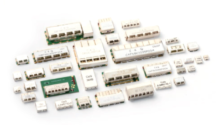
Ceramic Dielectric Filters:
Widely used in 4G, 5G, and 5G-A (5.5G) base stations, as well as in star network applications, demonstrating strong market relevance.​

1757003331378.png

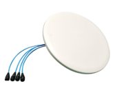
Ceramic Antennas:
Expansion from defense-focused applications to new areas such as indoor distributed antennas, vehicle-mounted antennas, and base station antennas.​

1757003352650.png

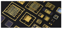
HTCC (High-Temperature Co-fired Ceramics) Development:
Established a complete in-house automated production line covering the entire HTCC process—from design and material preparation to sintering, metallization, brazing, testing, and analysis.
Developed 8 mature ceramic formulas (e.g., 92/95/96/99 alumina) and is researching high-thermal-conductivity aluminum nitride ceramics.
Achieved ultra-fine manufacturing capabilities: minimum single layer thickness of 0.1mm, aperture of 0.1mm, line width of 50μm, and line spacing of 50μm—suitable for high-precision components.
Completed development and small-batch delivery of various HTCC packaging products (e.g., microwave SIP, infrared tube shells, CMOS, optocouplers, CPGA, CBGA, etc.), with some already in customer use or mass production.
Successfully delivered several DPC ceramic substrates for verification.​

1757003372926.png

Thin-Film MEMS and Composite Ceramics:
Thin-film semiconductor circuits have entered mass production.
Composite ceramics (porous ceramics, aluminum-based silicon carbide, metal-ceramic composites) are being applied in heat dissipation substrates, 3C device housings, and lightweight braking systems for new energy vehicles—some products have already completed sample delivery.

Core Technologies & Material Capabilities:
Over 170 dielectric ceramic powder formulas developed; more than 80 commercially applied.
Dielectric constants range from 4 to 150 with tunable temperature coefficients, meeting needs for frequencies below 110GHz.
Full in-house production capability from raw powder to finished components, supporting flexible, customized manufacturing.​


Please, Log in or Register to view URLs content!
 

tokenanalyst

Brigadier
Registered Member

Gallium Ren Semiconductor's 8-inch gallium oxide substrate has been tested and is of internationally leading quality!.​

The 8-inch gallium oxide substrate of Hangzhou Gallium Ren Semiconductor Co., Ltd. (hereinafter referred to as "Gallium Ren Semiconductor") passed the inspection of well-known domestic and foreign institutions and jointly released the test results.

Third-party testing results indicate that the full width at half maximum (FWHM) of the XRD rocking curve for the 8-inch substrate is less than 30 arcsec , reaching internationally leading standards. The introduction of high-quality 8-inch gallium oxide substrates marks the full acceleration of gallium oxide industrial applications and a significant milestone in the industry's development.

According to the test results of Shenzhen Pinghu Laboratory, the test sample was an 8-inch gallium oxide substrate, with a total of 5 points taken. The half-height width of the XRD rocking curve test result was: 22~26 arcsec.

Please, Log in or Register to view URLs content!
 

tokenanalyst

Brigadier
Registered Member

Domestic GaN has made new breakthroughs.​


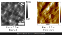
On September 3, Jingzhan Semiconductor revealed on its official Weibo that they announced the growth results of 6-inch N-face GaN materials for the first time through the dual combination of "substrate angle design" and "impurity suppression process", and successfully achieved the industry's best level of surface roughness of N-face GaN materials as low as 2nm.Jingzhan Semiconductor stated that N-face GaN has an opposite polarity direction compared to traditional Ga-face GaN ((0001) plane), thus exhibiting unique physical properties, including: better confinement of the two-dimensional electron gas (2DEG) in the heterojunction structure and lower ohmic contact resistance; the presence of spontaneous polarization electric field and semi-polar plane, making it suitable for low-voltage, high-frequency devices and optoelectronic devices.

However, there are two major difficulties in growing N-face GaN: first, the traditional N-face GaN positive axis growth is prone to surface aggregation due to the low transition ability of Ga atoms, which restricts the flatness of material growth; second, due to the special nature of the N-face, the background impurity Si and O concentrations are an order of magnitude higher than those on the Ga-face under the same growth conditions, which leads to leakage.

Therefore, Jingzhan Semiconductor optimized the AlN nucleation mechanism and precisely controlled the off-angle of the 6-inch SiC substrate to improve the N-face GaN crystal quality (GaN(002)<350 arcsec, GaN(102)<400 arcsec) and surface morphology (RMS~2nm), and controlled the background doping concentration below the SIMS detection line, successfully preparing N-face GaN materials with high crystal quality, low dislocations, and high surface flatness.​

1757005042286.png

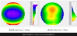
At the same time, Jingzhan Semiconductor has controlled the warpage of 6-inch epitaxial wafers to within 30 µm by optimizing different growth parameters, reaching the industry-leading level.

1757005125947.png

Please, Log in or Register to view URLs content!
 

tonyget

Senior Member
Registered Member
Please, Log in or Register to view URLs content!

Hanwha Semitec wins bid for BOE's microLED mounter.

Hanwha Semiconductor will supply micro light-emitting diode (LED) mounter equipment to BOE.

According to China Bidding on the 2nd, Hanwha Semitec was the sole bidder and won the bid for four units of chip mounter equipment ordered by Zhuhai BOE MLED (Micro LED) Technology. Bidding for the project began at 10:00 AM on the 29th of last month, and the deadline for results announcement was the 1st of this month.

Hanwha Semiconductor responded, "It is true that we participated in the bidding and won the bid," but added, "It is difficult to disclose the equipment model name or specific usage."

A mounter is a device that attaches components, such as semiconductor chips or LEDs, to specific locations on a printed circuit board (PCB). Unlike semiconductor packaging, which individually packages chips, chip mounters mount chips directly onto the circuit board. This is called the COB (Chip on Board) method.

BOE HC Semiconductor (Huacan Optoelectronics) has a 6-inch wafer-based micro LED production base in Jinwan District, Zhuhai, China. The chip mounter announced for bidding is expected to be supplied there.

Micro LED chips are less than 100 micrometers (㎛) in size. Ultra-precision equipment is required to secure them onto the board. Reducing the gap between chips can achieve sharper image quality.

An industry insider said, "The mounter equipment that Hanwha Semitec will supply is presumed to be the Decan F2 or XM5 series." Hanwha Semitec's chip mounter Decan F2 can precisely place chips within a margin of error of 40 µm, and the XM5 can do so within a margin of error of 22 µm.

Another official explained, "Chip mounters are not high-end equipment and the orders are large," adding, "The order amount will not be large."
 
Top