Shanghai Institute of Microsystem and Information Technology has made progress in large-scale fabrication technology of nanoscale vacuum channel devices
Vacuum channel electronics (VCEs) utilize a vacuum gap as their device channel, boasting electron mobility superior to all other semiconductor devices. They meet the demands of high-frequency communications, high-fidelity analog circuits, and applications in extreme environments such as high temperatures and strong radiation. In recent years, VCEs have become a research hotspot for post-Moore components. However, existing VCEs typically utilize methods such as electron beam lithography and focused ion beam etching to fabricate their nanochannels, which lack compatibility with CMOS processes, making large-scale fabrication and application difficult.
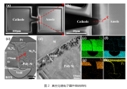
Shanghai Institute of Microsystem and Information Technology has developed a CMOS-compatible, large-scale fabrication method for nanoscale vacuum channel electronic devices using chemical mechanical polishing (CMP) combined with selective wet etching. This approach enables precise control over nanochannel formation on silicon-on-insulator (SOI) substrates.
the National Key Laboratory of Integrated Circuit Materials at the Shanghai Institute of Microsystem and Information Technology, Chinese Academy of Sciences, proposed a novel vacuum channel electronic device integration scheme combining chemical mechanical polishing (CMP) and selective wet etching. Based on a SOI substrate, the team successfully fabricated a prototype device with a 14 nm vacuum channel, achieving a low turn-on voltage (1.8 V) and a high emission current (70 nA at 5 V, T = 300 K).


