You are using an out of date browser. It may not display this or other websites correctly.
You should upgrade or use an alternative browser.
You should upgrade or use an alternative browser.
Chinese semiconductor thread II
- Thread starter vincent
- Start date
Industry first: HKC achieves breakthrough in micro-pitch LED large screen technology, integrating red, green and blue colors on a single chip
on February 17 that HKC announced today that it has made a breakthrough in the field of high-end displays, successfully completing the research and development of the world's first silicon-based GaN single-core integrated full-color Micro LED chip for application in the field of micro-pitch LED large-screen direct display.
This technology is jointly developed based on the SiMiP chip of Li-Ion Semiconductor , which improves production efficiency and display effects, and is claimed to have pushed China into the "global forefront" in the field of micro-pitch LED large-screen direct display technology.
Yongsi Electronics' high-end packaging technology layout: DiFEM module packaging technology achieves breakthrough in ultra-thin size.
As an important form of RF front-end modularization, DiFEM module can receive and process multiple signals by integrating RF switches and filters, which can reduce the size while improving integration and performance, meeting the needs of mobile smart terminal products. Innovation in DiFEM module packaging technology is one of the key factors in promoting the performance of communication equipment.
DiFEM module packaging achieves ultra-thin size, leading industry innovation
Yongsi Electronics has achieved breakthrough progress in the field of DiFEM module packaging. By using FCLGA packaging technology, RF switches and multiple filter chips are highly integrated together to achieve an ultra-thin package size.
● Selective cavity technology:
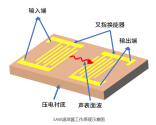
Yongsi Electronics has integrated a surface acoustic wave filter (SAW filter) in the packaging module, which has the advantages of stable performance, high operating frequency, and good frequency selection characteristics. The principle of this filter is that the input end converts the electrical signal into an acoustic signal through the piezoelectric effect and propagates on the surface of the medium, and the output end converts the acoustic signal into an electrical signal through the inverse piezoelectric effect. The mutual conversion process of electrical energy and mechanical energy is realized by the interdigital transducer (IDT). According to the working principle of the surface acoustic wave filter, it requires a cavity to work properly. The cavity structure is also a determining factor affecting the key indicators of the integrated surface acoustic wave filter RF module, such as size, cost, and performance. At present, Yongsi Electronics uses selective cavity technology in the entire module packaging to simultaneously realize the entire cavity structure at the bottom of the filter chip, and the bottom of the RF switch chip is 100% filled.
Yongsi Electronics has also studied multi-chip combination solutions, combined materials and processes, to achieve a better chip mounting sequence, and ultimately solved the challenges brought by mechanical force and thermal stress in the multi-chip packaging process. Surface mounting technology can be used to integrate 3-8 filter chips and 2 RF switch chips in a single module.

Weiqin Technology received tens of millions of yuan in Pre-A round financing for mass production and market expansion
3D vision sensor manufacturer "Weiqin Technology" has recently completed its Pre-A round of financing, with a financing amount of tens of millions of RMB, and the investor is Xiamen Hi-Tech Investment. This round of financing will be used for mass production of high-precision sensors and overseas market expansion. Founded in 2013, Weiqin Technology focuses on the research and development of core machine vision algorithms, sensors and software systems. It is an integrated hardware and software solution provider in the field of industrial inspection. Based on its independent technological accumulation, it has launched a code-free visual inspection platform, 3D line laser profile sensor and AI inspection system, covering 2D/3D visual inspection, high-precision measurement and industrial quality inspection and other scenarios. Its solutions have been implemented in 3C, lithium batteries, military industry, semiconductors and other fields. In terms of the team, Weiqin Technology founder Lin Shaobin has more than ten years of experience in machine vision. The core members include doctors from the Chinese Academy of Sciences and many industry experts. R&D accounts for 60%, and it holds more than 40 patents and intellectual property rights.
Weiqin Technology's self-developed MTD-L series 3D line laser profile sensors have a maximum repeatability of 0.1 microns and a scanning frequency of 30KHz, which is 100% higher than similar products (15KHz). It is suitable for high-speed inspection scenarios, but the unit price is much lower than similar products of foreign friends. This cost advantage comes from two technological innovations: first, through the optimization of optics, algorithms and hardware architecture, the integrated design of sensors is realized, and the hardware cost is reduced by 50%; second, it is equipped with built-in 3D detection software, and customers do not need to purchase additional detection systems.
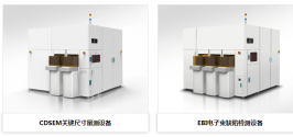
CDSEM for SiC-GaN chips.
Suzhou Sishi Technology Completes Hundreds of Millions of Yuan in Series A Financing
SiVision Technology, a leading company in semiconductor front-end electron beam measurement equipment industry solutions, has successfully completed a round of financing of several hundred million yuan. This round of financing was jointly invested by Jucheng Investment, Yida Capital, Guofa Venture Capital, Xiangcheng Financial Holdings and other institutions. Old shareholders continued to make additional investments, and Shanyun Capital served as the exclusive financial advisor for this round.
Founded in 2021, SiVision Technology is led by world-renowned technical experts in the electron beam field and co-founded by several returnee doctors. The company focuses on an extremely critical field in domestic semiconductor front-end equipment that faces "bottleneck" problems, namely the application of electron beam quantity detection technology in front-end wafer quantity detection. At present, the company's first CDSEM equipment has been put into use in the Fab plant for more than a year, with a production capacity of more than 500,000 pieces. It has successfully passed various stages of mass production and stress testing, and has begun to be sold in batches. At the same time, the upgraded version of CDSEM for domestic 6/8-inch (including three and a half generations) customers has completed product finalization and is in an intensive verification and testing stage. It is expected to become the main product sold in the market in 2025. In addition, the 12-inch CDSEM and electron beam defect detection equipment (EBI) that meet the needs of high-end processes have been integrated and will soon be launched on the market.
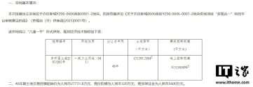
SMIC Beijing Phase II industrial land transaction, the total investment of the planned project is not less than 50 billion
The construction unit of the survey results report of Block 0001 of YZ00-0606 in Yizhuang New Town is shown as SMIC Beijing Integrated Circuit Manufacturing (Beijing) Co., Ltd.
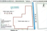
The construction unit of the survey results report of Block 0001 of YZ00-0606 in Yizhuang New Town is shown as SMIC Beijing Integrated Circuit Manufacturing (Beijing) Co., Ltd.


Last edited:
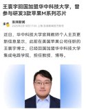
Wang Huanyu is a top chip developer. To be honest, he deserves applause for returning to Huazhong University of Science and Technology. But if he is willing to return to China's semiconductor industry, he may shine even brighter. Huawei, Tencent, Alibaba, Deepseek, DJI, Xiaomi, Baidu... a bunch of top technology companies are vying for him!
According to The Paper:
His full-time job at Apple is high-performance and low-power CPU design. Wang Huanyu has participated in the development of three Apple M series chips, of which the world's first 3nm Apple M3 series chip and Apple M4 series chip have been released and marketed.
Wang Huanyu has published more than ten papers in well-known computer engineering journals and conferences such as IEEE TCAD, IEEE TVLSI, IEEE/ACM ISLPED as the only first author, and has been granted two US patents.
He has served as a reviewer for many well-known computer engineering journals and conferences such as IEEE TC, IEEE TCAD, IEEE TVLSI, IEEE HOST, etc. He has participated in many scientific research projects such as DARPA and NSF in the United States, with a project amount of more than 8 million US dollars.

Last edited:
With an investment of 12 billion yuan, the Pioneer Compound Semiconductor R&D and Production Base Project aims to be put into production by the end of the year
According to the Yangtze River Daily, four production plants of the Pioneer Compound Semiconductor R&D and Production Base Project have been built recently, two of which have been capped and the other two are being poured. It is reported that the entire project will strive to be put into operation by the end of 2025. In the future, semiconductor substrates and epitaxial materials will be produced from these four production plants, which will effectively strengthen the supply chain of optical communications and laser industries in Optics Valley.
It is reported that the project is located south of Gaoxin 6th Road and east of Guanggu 5th Road, with a construction area of 260,000 square meters and a total of 19 buildings, including a research and development center, a production dispatching center, an office building, etc. It strives to be completed and put into use by the end of this year.
It is understood that Pioneer Technology Group Co., Ltd. is a global leader in rare metals. In March 2024, the project was settled in Optics Valley, with an investment of 12 billion yuan to build a high-end compound semiconductor material and chip industrialization base project. After the project is put into production, it will have the production capacity of gallium arsenide substrates, indium phosphide substrates, germanium wafers, tunable lasers and other products.
Total investment of 520 million! Shuoke Crystal Phase II project is fully put into production
Recently, Shuoke Crystal announced that its second phase of silicon carbide production line has been fully put into production, marking the further consolidation of the company's leading position in the field of silicon carbide materials. The commissioning of the second phase project will add 200,000 silicon carbide substrates to Shuoke Crystal's annual production capacity, further promoting its layout in the global silicon carbide market.
The production base of Shuoke Crystal is located in the Taiyuan Start-up Area (North Area) of Xiaohe Industrial Park, Shanxi Transformation and Comprehensive Reform Demonstration Zone. The project is divided into two phases. The total investment of the second phase project reached RMB 520 million, mainly to build a silicon carbide single crystal growth workshop in the original plot of China Electronics Technology (Shanxi) Silicon Carbide Materials Industrial Base, and purchase related production equipment and add new crystal growth equipment. The second phase expansion of the project will directly sell part of the production capacity, and the products further processed according to the order requirements will enter the existing workshop of the first phase for processing.
Shuoke Crystal Company stated that after the second phase of the project is put into production, the additional annual production of 200,000 silicon carbide substrates will include N-type silicon carbide single crystal substrates, 25,000 high-purity substrates and 1.3 tons of moissanite crystals. This increase in production capacity not only provides downstream customers with more diversified choices, but also further promotes the advancement of silicon carbide crystal technology.

