Chinese semiconductor thread II

tokenanalyst

Brigadier
Registered Member

The paper on storage and computing integrated chip of the Institute of Microelectronics was selected for ISSCC 2025 conference​

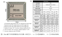
The team led by Researcher Zhang Feng from the National Key Laboratory of Integrated Circuit Manufacturing Technology has designed a transposable approximate and precise dual-mode floating-point storage and calculation integrated macro chip. Through the proposed cyclic weight mapping SRAM scheme, the chip can reuse the multiplication and addition units in forward and reverse propagation, and while realizing the transposition function, it greatly improves the energy efficiency and computing power density compared to the previous transposition storage and calculation integrated macro unit. Through the proposed signed fixed-point mantissa encoding method and vector granularity pre-alignment scheme, the chip realizes the compatibility support of multiple floating-point and fixed-point number systems, and has a smaller precision loss than the traditional coarse-grained floating-point pre-alignment scheme.

Through the proposed approximate and precise dual-mode multiplication and addition circuit design, the chip can turn on the approximate mode in the reasoning link with low precision requirements, thereby obtaining a 12% speed increase and a 45% energy consumption reduction, and can turn on the precise mode in the training link with high precision requirements to ensure no precision loss. The storage and calculation integrated macro chip is taped out under the 28nm CMOS process and can support BF16, FP8 floating-point precision operations and INT8, INT4 fixed-point precision operations. The average energy efficiency of BF16 floating-point matrix-matrix-vector calculations reached 48TFLOP/W, and the peak energy efficiency reached 100TFLOPS/W; the average energy efficiency of FP8 floating-point matrix-matrix-vector calculations reached 192.3TFLOP/W, and the peak energy efficiency reached 400TFLOPS/W. This research result provides new ideas for storage-computing integrated architecture chips used for edge training.

The above work was selected for ISSCC 2025 with the title of " A 28nm 192.3TFLOPS/W Accurate/Approximate Dual-mode Transpose Digital 6T-SRAM Compute-in-Memory Macro for Floating-Point Edge Training and Inference ". Yuan Yiyang, a doctoral student at the Institute of Microelectronics, is the first author, and Zhang Feng, a researcher, and Li Xiaoran, an assistant professor at Beijing Institute of Technology, are the corresponding authors. This research result was supported by the Key R&D Program of the Ministry of Science and Technology, the National Natural Science Foundation, and the Strategic Priority Research Program of the Chinese Academy of Sciences.
1739565809097.png

Please, Log in or Register to view URLs content!
 

tokenanalyst

Brigadier
Registered Member

A fluorine-containing polymer and its preparation method and ArF immersion photoresist made from the polymer​

CN119285842A​

Ruihong Suzhou Electronic Chemicals Co ltd

Abstract​

The present application relates to the technical field of photolithographic materials, and specifically discloses a fluorine-containing polymer and a preparation method thereof, and an ArF immersion photoresist prepared using the polymer. A fluorine-containing polymer comprises, by mol%, 5-15 mol% of an A monomer, 55-80 mol% of a B monomer and 15-30 mol% of a C monomer, wherein the A monomer is a methacrylate monomer having a lactone side chain, the B monomer is a methacrylate monomer having a protective group on the side chain, and the C monomer is a methacrylate monomer having a fluorine-containing side chain. The preparation method comprises the steps of dissolving, heating reaction, purification, drying and the like. The fluorine-containing polymer of the present application can be used to prepare ArF immersion photoresist, can form a water-resistant layer with excellent hydrophobicity on the surface of the photoresist, has good compatibility with the ArF immersion photoresist, and significantly improves the development performance of the photoresist.​
 

tokenanalyst

Brigadier
Registered Member

A temperature fluctuation attenuator based on cascade system and optimized manufacturing method​

CN119002193A​

Zhejiang University ZJU

Abstract
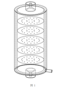
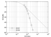
The present invention discloses a temperature fluctuation attenuator based on a cascade system and an optimized manufacturing method. The temperature fluctuation attenuator includes a main shell and a plurality of porous plates. The interior of the main shell is hollow to form a cavity structure. Each porous plate is a circular plate with small holes. The plurality of porous plates are arranged in parallel and spaced along the flow direction of the fluid. Each porous plate is perpendicular to the flow direction of the fluid and is used to block the flow and attenuate the fluctuation of the fluid. The optimized manufacturing method includes obtaining the volume V of the cavity structure, the diameter D of the porous plate, the density ρ of the ultra-clean fluid, the flow velocity v of the fluid and the time lag time τ, and then constructing a time lag model G(s) of the temperature fluctuation attenuator. Finally, the time lag model G(s) is optimized and solved to solve the number N of the porous plates, the number n of the small holes on the porous plates, and the aperture d of the small holes on the porous plates, thereby manufacturing the optimized temperature fluctuation attenuator. The present invention improves the attenuation performance of the attenuator under high-frequency temperature disturbance, which is beneficial to improving the temperature control accuracy of the lithography machine.

1739569941147.png1739569962156.png
 

tokenanalyst

Brigadier
Registered Member

ZOSON Piezoelectric MEMS Process Platform: Leading the Innovation of High-end Piezoelectric MEMS Technology​


According to MEMS Consulting, with the rapid development of science and technology, MEMS technology is becoming a key force in promoting changes in various industries. As a leader in the field of piezoelectric MEMS, Nanjing Zhouxun Microelectronics Technology Co., Ltd. (hereinafter referred to as Zhouxun Microelectronics ) has created the industry's top piezoelectric MEMS process platform with its world-leading aluminum nitride (AlN) and scandium-doped aluminum nitride (AlScN) process technology, providing strong support for the research and development and mass production of high-end micro-nano devices.

High-end process platform: full-chain R&D and mass production capabilities

The piezoelectric MEMS process platform of ZS Microelectronics is based on 6-inch wafers and is equipped with world-class equipment and a complete process chain, covering the entire process from R&D to mass production. The core advantages of the platform include:

Advanced equipment and technology

- Thin film deposition:
High-precision PVD sputtering system is used to ensure high-quality deposition of AlN and AlScN thin films.

- Lithography and Etching: Equipped with stepper lithography system and plasma etching system, supporting sub-micron patterning process.

- Chemical Mechanical Planarization (CMP): Achieve ultra-high flatness of film surface and improve device performance.

- Wafer testing and packaging: Integrate wafer ball implantation, thermal compression and ultrasonic flip-chip, test taping and other processes to ensure high reliability and consistency of products.

Full chain process integration

The platform seamlessly connects key process modules such as lithography, thin film deposition, etching, CMP, testing, and packaging to form a complete piezoelectric MEMS process chain. This highly integrated model not only improves process efficiency, but also provides flexible technical support for the development of complex devices.

Since its official operation in July 2021, Aeolus Microelectronics has provided process development and mass production services to many customers around the world, developed more than 50 products, and shipped more than 200 million units. Our platform has passed the ISO9001 quality system certification to ensure that the delivered products meet world-class standards. At the same time, we have established a complete customer intellectual property protection system to ensure that the business secrets of our partners are fully protected.

1739635055498.png

Please, Log in or Register to view URLs content!
 

tonyget

Senior Member
Registered Member
Please, Log in or Register to view URLs content!

SK Hynix to Exclude Chinese Semiconductor EDA… “Preemptive Response to Trump Regulations”

I used it for cheap, but the U.S. sanctions move
China-made SW Appropriateness review
I love this app but I can't wait to see if I can use it.

Increasing semiconductor design costs is inevitable

SK Hynix Emergency Semiconductor Electronic Design Automation(EDA) Software Made in China Went into check. Donald Trump's second-term government also talks about Chinese Software for Korean semiconductor companies It is reported that it will regulate its use and will spiral into proactive response.

According to the semiconductor industry on the 16th, SK Hynix is using China-made EDA software It has been confirmed that it is reviewing its appropriateness. EDA is used to design and validate system semiconductor integrated circuit (IC) designs With software, various circuit designs before making semiconductor chips It is used to simulate and predict results. As long as the chip is completed and then the defect is found, the entire amount must be discarded It's a kind of proactive program. ’Without EDA, there is no semiconductor design of the latest process' It's the reason.

This market is more than 70% by US companies such as Synopsis, Cadence, Siemens EDA I'm taking control. However, in recent years, the new China has poured "caustic EDA", and China's share has It's an increasingly rising trend. Empyrian, Primarius, Entasis, etc.are such companies. Samsung Electronics and SK Hynix, mainly made in the United States, have recently been made in China I'm writing together. Chinese companies blocked by U.S. exports include Samsung Electronics and SK Hynix This is due to the strengthening of sales.

SK Hynix is in an emergency check on the Trump Government's additional China sanctions The contrast aspect is large. At the end of last year, Empirian Korea, a Korean branch of EDA in China, traded to the United States The analysis that the designation of a limited company also affected.

In the industry, SK Hynix will stop using EDA made in China I'm expecting. Don't have an uncomfortable relationship with the United States, the "big hand" of the semiconductor market That's why it's supposed to be. The proportion of EDA made in China is not large, which is also a part of this observation. From 2022, we will use EDA made in China such as Empyrian, Primarius and Entasis The industry expected that Samsung Electronics will also make the same decision.

If Samsung Electronics and SK Hynix cut off Chinese EDA, the U.S. dependence The higher the cost of semiconductor design, the higher the cost of semiconductor design. This is because U.S.-made EDA is more than twice as expensive as Chinese-made EDA. If the supply chain is unified in the U.S., prices are likely to rise further There are. “The price is less than half of the performance similar to the U.S.-made EDA, " an industry official said Samsung Electronics and SK Hynix will eventually design when made in China is exited Related costs will rise, " he expected.

SK Hynix officials said, “The time of renewal of the EDA contract made in China has come We're reviewing whether to use it."
 

tokenanalyst

Brigadier
Registered Member

Zhejiang YuYue's 600,000-ton annual optical film project officially started production.​


The "10 billion-level" investment project in Keqiao District, Shaoxing, produced another fruitful result - the 600,000-ton optical film project of Zhejiang Yuyue New Materials Co., Ltd. in Keqiao Economic Development Zone was officially put into production. The official launch of the project marks that domestic optical films have broken through foreign technical barriers and achieved large-scale mass production, entering a new historical node, and also injecting more energy into Shaoxing Keqiao District to achieve the transformation and leap from traditional manufacturing to new quality productivity.

Production lines are in operation, equipment is in operation, and personnel are in place... Walking into the production workshop of the Yuyue Optical Film Material Manufacturing Project, the winding pipes are arranged in an orderly manner like the roots of an old tree. Under the skilled operation of technicians, huge kettles are working at full capacity. The on-site links are tense and orderly, playing an exciting movement of progress in the new year. It is reported that the project took only 17 days from the withdrawal of land to the start of construction, and the construction lasted more than 20 months. The first batch of production lines was officially ignited and put into production today!

Please, Log in or Register to view URLs content!
 
Top