You are using an out of date browser. It may not display this or other websites correctly.
You should upgrade or use an alternative browser.
You should upgrade or use an alternative browser.
Chinese semiconductor thread II
- Thread starter vincent
- Start date
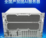
Jingjiawei releases domestically produced AI reinforced server, ready to use out of the box!
In the wave of rapid iteration of AI technology, DeepSeek, a domestic open source large model, has emerged with disruptive innovation. Through autonomous algorithm iteration, deep optimization of computing power, multi-modal co-evolution and open source ecosystem construction, it breaks through the dependence on traditional technology paths and drives domestic AI to achieve leapfrog development from technology catching up to ecosystem leadership.
Jingjiawei quickly integrated into the DeepSeek large-model localization ecosystem and launched a domestically produced reinforced AI server with a pre-installed DeepSeek-R1 model, promoting intelligent transformation in various industries with its own controllable computing infrastructure.
Features
Domestic Ecology
The server is independently designed based on 100% domestic modules and components. The operating system and software stack are deeply integrated with the domestic ecosystem. It is pre-installed with the domestic DeepSeek-R1 open source large model to achieve end-to-end independent control from chip-level hardware to system-level software.
Ready to use
The server has built-in Deepseek-R1 1.5B ~ 70B distillation model, which supports interactive demonstration of large models with zero configuration. Developers can quickly call preset model interfaces to enable vertical scenarios such as knowledge graph construction and intelligent coding assistance, accelerating the implementation of industry AI solutions.
Super computing power
A single server can be equipped with up to 2000 TOPS computing power and 256GB high-speed video memory. A single server can drive the highest DeepSeek-R1 70B distillation model inference, and can simultaneously deploy multiple DeepSeek-R1 distillation models with different parameters, supporting up to 200+ users with high concurrent access, meeting the usage scenarios of a team of 1,000 people. An elastic computing power cluster is built through the RoCE lossless network, with reserved deployment capabilities for models with hundreds of billions of parameters (compatible with the full-parameter version of DeepSeek-R1 671B).
Wide temperature reinforcement
Through reinforced design and built-in redundant power supply, it has the characteristics of resistance to strong vibration, electromagnetic shielding, and three protections (moisture-proof/dust-proof/corrosion-proof), ensuring continuous and stable operation under complex working conditions in special industries.
The in-depth collaboration between Jingjiawei and DeepSeek, with the "hardware and software integration" of the domestically produced hardware base and the independent large model, not only strengthens the security line of defense of the AI computing infrastructure, but also provides a reliable intelligent foundation for thousands of industries with an out-of-the-box technology system.
In the future, Jingjiawei will continue to deepen its research in the fields of computing power optimization, large-model software and hardware collaborative adaptation, and special scenario technology breakthroughs, accelerate the transition from "usable" to "easy to use", and work with ecological partners to improve the domestic AI technology map, providing higher performance and more widely compatible autonomous and controllable solutions for ultra-large-scale model deployment and full-scenario industry empowerment.


Xuantian Technology Semiconductor Smart Factory, Production Line and Equipment Industrialization Project Successfully Capped
On January 5, the capping ceremony of Xuantian Technology's semiconductor smart factory, smart production line and intelligent equipment industrialization project was successfully held in Pinghu! In the future, as Xuantian Technology's R&D and production base in the Yangtze River Delta, the project will echo with R&D bases in Shanghai, Hangzhou, Xi'an, Suzhou, Chengdu and other places, further improving overall production capacity and corporate competitiveness.
The successful completion of the project marks a new step for Xuantian Technology in independent innovation and large-scale production. As a high-tech enterprise focusing on Industry 4.0 and intelligent manufacturing system solutions, Xuantian Technology is committed to providing professional digital factory overall solutions for semiconductors, micro-assembly/electrical equipment/final assembly, automotive electronics/3C electronics, pharmaceuticals and other fields, and has won the trust of industry benchmark customers such as CRRC Group, Infineon, BYD, NARI, and China Electronics Technology Group Corporation. The construction period of this project is 10 months, covering a total area of 32.83 acres, and a new 47,000 square meters of factory buildings will be built, which will introduce various types of production and testing equipment.
This project is an important milestone in the company's development history. With its full implementation, the company will achieve a leapfrog increase in production capacity in the two key areas of smart production lines and precision semiconductor equipment, which will not only effectively meet the growing market demand, but also significantly shorten the product delivery cycle, significantly improve delivery efficiency, and provide customers with a better quality and more efficient service experience.
Changfei Quartz completes plant construction and equipment installation and is expected to be fully operational in the first half of this year
Recently, in the Changfei Technology Park on Guanggu 3rd Road, the construction of the Changfei Optical Quartz Components R&D and Industrialization Project is in full swing. At present, the project plant infrastructure and equipment installation have been completed as scheduled, and it is expected to be fully put into production in the first half of this year.
Changfei Quartz focuses on the research and development and manufacturing of high-end quartz materials. It independently masters a variety of international mainstream chemical vapor deposition, synthetic quartz preparation and other processes. Its products have the characteristics of high purity, bubble-free, high optical uniformity, etc., which can meet the stringent demands of optics, optical communications and other industries for high-end quartz materials.
In April 2023, the East Lake High-tech Zone signed an investment cooperation agreement with Changfei Quartz to build an optical-grade quartz component R&D and production base project, aiming to use independently developed technologies and equipment to expand the manufacturing of optical high-end quartz through the extension of the fiber-grade high-purity synthetic quartz manufacturing platform, and strive to achieve the industrialization and domestic substitution of optical quartz components. The project started construction in July of that year and was successfully capped in January last year.
"During the Spring Festival, the project construction team was doing the final debugging of the production line equipment, striving for full production in the first half of 2025!" said the relevant person in charge of the company.
Implementation of a dynamic gas lock mechanism reducing contamination in extreme ultraviolet cleanrooms.
Abstract
The dynamic gas lock (DGL) is an effective structure in extreme ultraviolet (EUV) lithography, designed to mitigate the diffusion of hydrocarbons from the wafer chamber to the optics chamber. This study presents a comprehensive DGL model that considers adsorption, desorption, and decomposition of hydrocarbons on the optical surface. Using the direct Monte Carlo method, we enhanced the dsmcFoam + solver to describe outgassing boundary contamination accurately. The model estimates the EUV loss rate and carbon deposition rate under various clean gas conditions (<50 Pa·L/s) and predicts a maximum EUV loss rate that does not exceed 0.25 %. We performed multi-objective optimization using the non-dominated sorting genetic algorithm II to optimize process parameters and yield solutions. Both experimental data and solutions confirm that our DGL model effectively inhibits pollution, achieving a maximum experimental inhibition rate of 76.53 %. The model and optimization method provides a multifactorial analysis for DGL studies with high accuracy due to comprehensive factor consideration. This approach can be applied to similar studies on multiphase flow in high vacuum environments, providing efficient and accurate data for industrial production.
Gpixel releases GLT5009BSI-DUV version to help semiconductor defect detection
On August 15, 2024, Gpixel released the Deep Ultraviolet (DUV) enhanced version of the time-delayed integration (TDI) CMOS image sensor GLT5009BSI. The product adopts advanced back-illuminated technology. Based on the visible light version of GLT5009BSI, the DUV version greatly improves the sensitivity in the UV range. Combined with the inherent high resolution, high sensitivity, high dynamic range, wide spectral response, low noise and other excellent performance of GLT5009BSI, the application field of the DUV version has been further expanded, providing more efficient and accurate detection support for applications such as semiconductor wafer defect detection and semiconductor material defect detection.
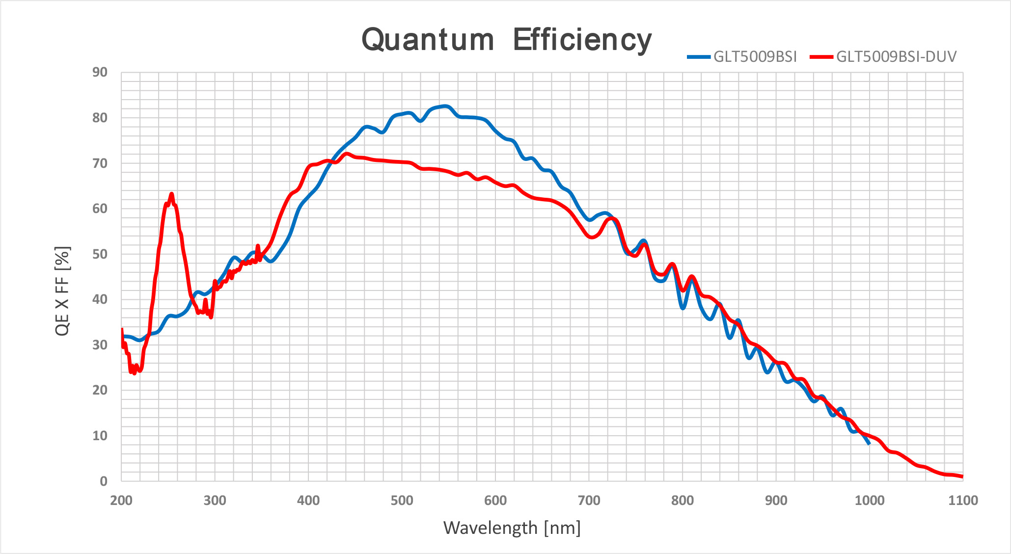
At present, most semiconductor wafer inspection systems use 266nm lasers. In order to meet the needs of wafer inspection at 266nm, Gpixel has optimized the structure of the ARC film system on the pixel layer on the wafer surface based on the GLT5009BSI visible light version, and improved the response of the TDI sensor in the DUV spectrum, so that its quantum efficiency in the 266nm band can reach more than 50%. The GLT5009BSI-DUV version of the chip not only ensures the detection efficiency with its extremely high line frequency, but also makes the detection system more sensitive.

The DUV version is the same as the visible light version, with a 5μm pixel design and a horizontal resolution of 9072 pixels. The chip has two integral spectrum bands, and its TDI integral levels are 256 and 32 respectively. Users can choose according to their usage requirements. GLT5009BSI-DUV has a full well of 16ke⁻ and a readout noise of 6e⁻, and its single-frame dynamic range is 68dB. The chip can also output two spectrum bands at the same time for high dynamic synthesis, further improving the dynamic range. The chip is also optimized for the problem of strong light overflow, and its anti-halo capability can reach 100x.
The GLT5009BSI-DUV version maintains the high line frequency characteristics of the visible light version. The chip can output up to 608kHz@10bit and 300kHz@12bit line frequencies. The chip also supports on-chip 1x2 pixel merging, which further improves sensitivity without losing line frequency.
The packaging information of the GLT5009BSI-DUV version is the same as that of the visible light version. Based on the visible light version, users can quickly integrate the DUV version of the chip without changing any hardware and software design. DUV products are available for ordering from now on .
At present, most semiconductor wafer inspection systems use 266nm lasers. In order to meet the needs of wafer inspection at 266nm, Gpixel has optimized the structure of the ARC film system on the pixel layer on the wafer surface based on the GLT5009BSI visible light version, and improved the response of the TDI sensor in the DUV spectrum, so that its quantum efficiency in the 266nm band can reach more than 50%. The GLT5009BSI-DUV version of the chip not only ensures the detection efficiency with its extremely high line frequency, but also makes the detection system more sensitive.
The DUV version is the same as the visible light version, with a 5μm pixel design and a horizontal resolution of 9072 pixels. The chip has two integral spectrum bands, and its TDI integral levels are 256 and 32 respectively. Users can choose according to their usage requirements. GLT5009BSI-DUV has a full well of 16ke⁻ and a readout noise of 6e⁻, and its single-frame dynamic range is 68dB. The chip can also output two spectrum bands at the same time for high dynamic synthesis, further improving the dynamic range. The chip is also optimized for the problem of strong light overflow, and its anti-halo capability can reach 100x.
The GLT5009BSI-DUV version maintains the high line frequency characteristics of the visible light version. The chip can output up to 608kHz@10bit and 300kHz@12bit line frequencies. The chip also supports on-chip 1x2 pixel merging, which further improves sensitivity without losing line frequency.
The packaging information of the GLT5009BSI-DUV version is the same as that of the visible light version. Based on the visible light version, users can quickly integrate the DUV version of the chip without changing any hardware and software design. DUV products are available for ordering from now on .
Beijing Haidian District releases new measures for the integrated circuit industry, with a maximum subsidy of 15 million yuan for a single enterprise
According to news from Beijing Haidian, on February 14, the "Zhongguancun Science City Integrated Circuit Tapeout Subsidy Application Guide" (hereinafter referred to as the "Application Guide") was officially released at the 2025 Haidian District Economic and Social High-Quality Development Conference. It is aimed at companies in Haidian District engaged in integrated circuit design business, and supports integrated circuit design companies to carry out multi-project wafers (MPW) or the first round of tape-outs (full mask) of engineering products. The maximum subsidy for a single company is 15 million.
According to the Application Guidelines, in terms of supporting integrated circuit design companies to carry out the first round of multi-project wafer (MPW) tape-outs, domestic companies will be rewarded no more than 50% of the product tape-out costs, with a maximum of RMB 3 million for a single company. Foreign companies will be rewarded no more than 30% of the product tape-out costs, with a maximum of RMB 2 million for a single company.
In terms of supporting integrated circuit design enterprises to carry out the first round of engineering product tape-outs (full mask), enterprises that carry out the first round of tape-outs (full mask) of advanced process (14nm and below) engineering products in China will be rewarded at a rate not exceeding 30% of the product tape-out costs, with a maximum of 8 million yuan for a single enterprise; enterprises that carry out the first round of tape-outs (full mask) of mature process (14nm and above) engineering products in China will be rewarded at a rate not exceeding 20% of the product tape-out costs, with a maximum of 5 million yuan for a single enterprise; enterprises that carry out the first round of tape-outs (full mask) of advanced process (14nm and below) engineering products abroad will be rewarded at a rate not exceeding 15% of the product tape-out costs, with a maximum of 5 million yuan for a single enterprise. In addition, if an enterprise has multiple products that meet multiple application conditions, it can apply at the same time, and the maximum reward amount for a single enterprise this year shall not exceed 15 million yuan.
Xingji Micro Equipment is overloaded with orders
The global demand for AI computing power has exploded, driving the accelerated upgrading and production increase of high-layer PCB boards and high-end HDI industries. In addition, driven by the expansion of the PCB industry chain to overseas, Xingji Micro Equipment (stock code: 688630) has relied on its technological advantages and international layout. The current order delivery plan has been scheduled to the third quarter of 2025. The company's production capacity is in an overloaded state, and the business prospects continue to improve. The company is making every effort to promote the construction of the second phase base, striving to put it into use in mid-2025 to ensure timely delivery.
AI computing power drives demand for high-end equipment
With the rapid development of AIGC (generative artificial intelligence) technology, high-performance computing hardware such as AI servers and OAM accelerator cards have significantly increased the demand for high-end products such as high-layer boards, HDI and IC substrates of PCBs. The LDI direct imaging MAS series and solder mask direct imaging MAS series of Xingji Micro-Equipment have been adopted by many leading customers due to their high precision and high efficiency, becoming the core equipment for manufacturing such high-end PCBs.
Successful overseas strategy boosts growth
Southeast Asia is gradually becoming a new hot spot for the expansion of the global PCB industry chain. Xingji Micro Equipment has seized this opportunity keenly, not only exceeding its overseas order target for 2024, but also actively expanding overseas markets, making overseas business an important engine for the company's performance growth. This pace will continue to lead the company to achieve faster growth in 2025.
Increase production capacity to meet market demand
In order to meet the growing market demand, Xingji Micro Equipment has significantly increased its production capacity in 2024, and its current capacity utilization rate is close to saturation. This proactive capacity expansion strategy ensures that the company can effectively respond to customer needs, while also laying a solid foundation for continued growth in the future.
Through its precise positioning and technological breakthroughs in the field of AI computing power, as well as its successful overseas layout, Xingji Micro Equipment has demonstrated a typical case of Chinese high-end equipment manufacturing companies going global. Looking to the future, Xingji Micro Equipment will continue to be committed to technological innovation and service optimization to create more value for customers.

Heavy Ion Induced SEUs and Layer Dependence in Dual-Deck 3D NAND Flash Memories
Institute of Modern Physics, Chinese Academy of Sciences, Lanzhou, ChinaSchool of Nuclear Science and Technology, University of Chinese Academy of Sciences, Beijing, China
Abstract:
3D NAND technology has garnered increasing attention within space applications as a focal point of commercial competition and industrial evolution in semiconductor memory. With the increase in the number of layers, dual-deck architecture is being gradually integrated into products to reduce process fluctuations and improve the electrical performance. However, it is essential to carefully evaluate the response of such new devices to radiation effects. In this study, the three-dimensional distribution characteristics of single-event upsets (SEUs) were investigated in 128-layer dual-deck 3D NAND Flash memory induced by heavy ion irradiation. By measuring the threshold voltage distribution of charge-trapping cells under different heavy ion conditions, the dependence of the number and size of multi-cell upsets (MCUs) on the linear energy transfer (LET) was analyzed and the underlying physical mechanisms of these radiation effects were explored. Additionally, the variation of SEU along the layer is closely related to the dual-deck structure and channel-hole etch process. This work provides important reference data for improving the reliability design of 3D NAND Flash devices in radiation environments.

