You are using an out of date browser. It may not display this or other websites correctly.
You should upgrade or use an alternative browser.
You should upgrade or use an alternative browser.
Chinese semiconductor thread II
- Thread starter vincent
- Start date
@FairAndUnbiased Good stuff.
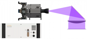
Back-end lithography applications in the semiconductor, MEMS, LED chip, power device and microfluidics industries will use a variety of mask alignment systems . Manual, semi-automatic and fully automatic mask aligner systems are available to meet the requirements of any production environment.
Hongke UVLED ultraviolet light source solutions (ALE/1, ALE/1C and ALE/2) have been successfully integrated into various mask alignment systems and can produce excellent results in contact exposure and projection exposure applications. Excellent uniformity , excellent collimation characteristics (<2°), high resolution down to 0.7μm and high surface radiated power have been seen on 4, 6, 8 and 12-inch substrates .
Broadband stepper systems play a vital role in advanced packaging applications such as fan-out wafer-level packaging (FOWLP), wafer-level chip-scale packaging (WLCSP) or through-silicon vias (TSV). Complex microstructures such as MEMS or LEDs are important examples of those fabricated on highly specialized stepper devices.
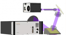
Hongke Broadband ALE/1 and ALE/1C light sources combine individual LED modules around the i-line, h-line, and g-line into a single light path, allowing complete control of the spectral composition of broadband exposure in the 350-450 nm range, enabling implementations as low as Resolution in the 1μm or even submicron range provides higher radiation output . By using Hongke light source solutions, you can have complete flexibility in selecting photosensitive advanced packaging materials that may need to be applied in the process, replacing or replacing any traditional high-power mercury arc lamps up to 1kW or higher, providing excellent system throughput.
Hongke Light Source Solutions In Semiconductor Manufacturing Process
The semiconductor industry relies on ultraviolet high-power radiation (i-line: 365 nm, h-line: 405 nm, and g-line: 436 nm) to produce complex microscopic circuits such as ICs, LCDs, PCBs, and MEMS in various photolithography, exposure, and development processes structure. Thanks to the technical and cost advantages of LED, the semiconductor manufacturing field is moving away from the long-standing traditional discharge mercury lamp technology and choosing UVLED technology as an ideal solution.Hongke UVLED ultraviolet light source provides stable and ultra-high power UV radiation output, with a maximum output power of up to 80W . It has long life and cost advantages. It does not require additional cooling time and is ready to use. It replaces the traditional light box structure and is no longer needed. Main beam folding mirror and heat sink to absorb radiation above 450nm below the shutter and filter components.
Many lithography applications rely on broadband exposure to radiation including the i, h, and g lines (365/405/435 nm). Hongke UVLED ultraviolet light sources provide very similar broadband spectral output , so upgrading existing photolithography processes to UVLED exposure systems no longer requires too much adjustment and operation. In addition to the broadband UVLED exposure units, output configurations with single peak (365 nm) or double peak wavelengths (365/405 nm and 405/435 nm) are also available.
Many lithography applications rely on broadband exposure to radiation including the i, h, and g lines (365/405/435 nm). Hongke UVLED ultraviolet light sources provide very similar broadband spectral output , so upgrading existing photolithography processes to UVLED exposure systems no longer requires too much adjustment and operation. In addition to the broadband UVLED exposure units, output configurations with single peak (365 nm) or double peak wavelengths (365/405 nm and 405/435 nm) are also available.
Mask Alignment System
Back-end lithography applications in the semiconductor, MEMS, LED chip, power device and microfluidics industries will use a variety of mask alignment systems . Manual, semi-automatic and fully automatic mask aligner systems are available to meet the requirements of any production environment.
Hongke UVLED ultraviolet light source solutions (ALE/1, ALE/1C and ALE/2) have been successfully integrated into various mask alignment systems and can produce excellent results in contact exposure and projection exposure applications. Excellent uniformity , excellent collimation characteristics (<2°), high resolution down to 0.7μm and high surface radiated power have been seen on 4, 6, 8 and 12-inch substrates .
(2.3) Ultra-High Power Output Exposure
Broadband Stepper System
Broadband stepper systems play a vital role in advanced packaging applications such as fan-out wafer-level packaging (FOWLP), wafer-level chip-scale packaging (WLCSP) or through-silicon vias (TSV). Complex microstructures such as MEMS or LEDs are important examples of those fabricated on highly specialized stepper devices.
Hongke Broadband ALE/1 and ALE/1C light sources combine individual LED modules around the i-line, h-line, and g-line into a single light path, allowing complete control of the spectral composition of broadband exposure in the 350-450 nm range, enabling implementations as low as Resolution in the 1μm or even submicron range provides higher radiation output . By using Hongke light source solutions, you can have complete flexibility in selecting photosensitive advanced packaging materials that may need to be applied in the process, replacing or replacing any traditional high-power mercury arc lamps up to 1kW or higher, providing excellent system throughput.
(3.2) Medium Power Output Exposure
It is way more complicated than that. Miniaturization has inherent speed and power efficiency benefits. The changes of HBM3 is not limited to I/O either. It adds new commercial functions and changes the clocking architecture.I do not get it. Isn't the difference between HBM2E and HBM3 about the I/O? The process just basically influences memory density and hence price.
China, sooner or later, has to match the foreigners in efficiency. Both to export and for its own productivity. It is not about CXMT earning money.But I doubt CXMT would have much competition in the HBM market. At least not in China they wouldn't. So price would be a small factor.
Those are not the same. Though stacking for HBM is not harder either.The fact that HBM is also basically a stacked memory type might mean someone like YMTC could also try to tackle that. At least they have experience with stacking for VNAND. Xtacking uses wafer bonding with TSV.
80W photon output is monstrous.@FairAndUnbiased Good stuff.
Hongke Light Source Solutions In Semiconductor Manufacturing Process
The semiconductor industry relies on ultraviolet high-power radiation (i-line: 365 nm, h-line: 405 nm, and g-line: 436 nm) to produce complex microscopic circuits such as ICs, LCDs, PCBs, and MEMS in various photolithography, exposure, and development processes structure. Thanks to the technical and cost advantages of LED, the semiconductor manufacturing field is moving away from the long-standing traditional discharge mercury lamp technology and choosing UVLED technology as an ideal solution.Hongke UVLED ultraviolet light source provides stable and ultra-high power UV radiation output, with a maximum output power of up to 80W . It has long life and cost advantages. It does not require additional cooling time and is ready to use. It replaces the traditional light box structure and is no longer needed. Main beam folding mirror and heat sink to absorb radiation above 450nm below the shutter and filter components.
Many lithography applications rely on broadband exposure to radiation including the i, h, and g lines (365/405/435 nm). Hongke UVLED ultraviolet light sources provide very similar broadband spectral output , so upgrading existing photolithography processes to UVLED exposure systems no longer requires too much adjustment and operation. In addition to the broadband UVLED exposure units, output configurations with single peak (365 nm) or double peak wavelengths (365/405 nm and 405/435 nm) are also available.
Mask Alignment System
Back-end lithography applications in the semiconductor, MEMS, LED chip, power device and microfluidics industries will use a variety of mask alignment systems . Manual, semi-automatic and fully automatic mask aligner systems are available to meet the requirements of any production environment.
Hongke UVLED ultraviolet light source solutions (ALE/1, ALE/1C and ALE/2) have been successfully integrated into various mask alignment systems and can produce excellent results in contact exposure and projection exposure applications. Excellent uniformity , excellent collimation characteristics (<2°), high resolution down to 0.7μm and high surface radiated power have been seen on 4, 6, 8 and 12-inch substrates .
(2.3) Ultra-High Power Output Exposure
Broadband Stepper System
Broadband stepper systems play a vital role in advanced packaging applications such as fan-out wafer-level packaging (FOWLP), wafer-level chip-scale packaging (WLCSP) or through-silicon vias (TSV). Complex microstructures such as MEMS or LEDs are important examples of those fabricated on highly specialized stepper devices.
Hongke Broadband ALE/1 and ALE/1C light sources combine individual LED modules around the i-line, h-line, and g-line into a single light path, allowing complete control of the spectral composition of broadband exposure in the 350-450 nm range, enabling implementations as low as Resolution in the 1μm or even submicron range provides higher radiation output . By using Hongke light source solutions, you can have complete flexibility in selecting photosensitive advanced packaging materials that may need to be applied in the process, replacing or replacing any traditional high-power mercury arc lamps up to 1kW or higher, providing excellent system throughput.
(3.2) Medium Power Output Exposure
Mercury lamp is <10% efficient with isotropic emission, ends up something like 0.6% efficiency on wafer.
UV LED is 27% power efficiency for near monochromatic light and already nearly collimated.
At least electricity cost are going down, no heat waste for better cooling and more compact tools.80W photon output is monstrous.
Mercury lamp is <10% efficient with isotropic emission, ends up something like 0.6% efficiency on wafer.
UV LED is 27% power efficiency for near monochromatic light and already nearly collimated.
50k wpm is a lot
View attachment 125329
Doing some rough calculation here. I think 500k Ascend chips is a lot. I did some calculation assuming they are making Ascend-920 (and computation increases to 600 TFLOPS FP16), that'd be 300 EFLOPS a year, which is way more than what they are adding right now
But contrast that with NVidia who are planning on 2 Million H100 chips for 2024.
0.5-1 Million Ascend 920 chips (which are supposed to be higher or comparable in performance) doesn't sound excessive.
Given that these chips are being sold for $40K, the profit margins should be tremendous.
The H100 is estimated to cost $3300. An Ascend at 50% more would be $5000.
No other chips match this level of profitability
And you can see the Ascend chips require very little overall wafer capacity compared to the smartphone chips.
Finally confirmation of Guowang’s own FlexWave, where lens aberration is corrected thermally by a TFT LCD-like film. ASML’s FlexRay for illumination and FlexWave for projection lens are key techs for advanced node DUV.
Confirmation of micro mirror array MEMS design similar to FlexRay developed by Raewang, Guowang’s Shanghai subsidiary. Critical for SMO part of computational litho. These optical techs, along with planar grating and maglev stage, enable duv below 28nm.
SMEC or SAI manufacture the micromirror arrays and looks like Guowang is assembling the whole thing.
Confirmation of micro mirror array MEMS design similar to FlexRay developed by Raewang, Guowang’s Shanghai subsidiary. Critical for SMO part of computational litho. These optical techs, along with planar grating and maglev stage, enable duv below 28nm.
The guy in the post talk about the micromirror array illuminator of the lithography that due patterning and overlay reasons has to send the light to the wafer in different shapes for efficiency because sadly for us nature decided to slap fab workers in the face and be a wave and particle at the same time, so you have to find workarounds to increase the resolution of your optical fabrication tools.
View attachment 125095
The I saw this guy tweet bragging about the FlexRay MEMS <lets keep in mind that> micromirror array. Pretty neat technology to be honest the closest thing to maskless DUV lithography and also one the early use of advance packaging.
"FlexRay and Tachyon SMO are two key, complementary ingredients in ASML’s holistic lithography portfolio."
View attachment 125097
Back in the day when the first SMEE ArF scanner was out they where using microlenses.
View attachment 125096
I thought to myself wow, they got me there, who is supplying this in China? Well China has two big MEMS manufacturers SAI micro and SMEC, they have advance packaging companies and they have fabs that can make ASIC chips 28nm down to 7nm. All boil downs to logic.
So yes looks like that China has narrow down on this technology and they recently published a paper discussing this tech.
View attachment 125098
Statement of one the micro-mirror mems manufacturers in China:
"international operation of high-end integrated circuit wafer foundry manufacturers, but also domestic with independent intellectual property rights and master the core semiconductor manufacturing technology of the characteristics of the process of professional wafer manufacturers. The company has many pilot platforms and mass production factories at home and abroad, and its business covers the world. Its service customers include internationally renowned DNA/RNA sequencer, lithography machine, computer network and system, silicon photon, infrared, wearable equipment, new medical equipment, automotive electronics and other giant manufacturers, as well as leading enterprises in the sub industry, The product range covers many fields such as communication, biomedical, industrial automobile, consumer electronics, etc. At the same time, the company is building advanced wafer-level packaging and testing capabilities, is committed to providing customers with systematic high-end manufacturing services from process development, wafer manufacturing to packaging and testing, and strives to develop into a well-known semiconductor manufacturing leader with international operations. "
holistic lithography:
View attachment 125100


