Chinese semiconductor thread II

tokenanalyst

Brigadier
Registered Member

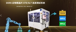
Huanghu Test received 100 million yuan in Series B financing and has focused on DRAM memory testing for more than 30 years​

Huanghu Test Technology (Shenzhen) Co., Ltd. (referred to as: Huanghu Test) completed a round B financing of 100 million yuan, led by CICC Capital, Wanlian Guangsheng, Xincong Yuanchen, Ruifa Fund, etc. participated in the investment, and the old shareholder Wanwuyi made additional investment.​
1707821775445.png


Official news from Huanghu Test shows that it has focused on the field of memory high-speed test equipment for more than 30 years and is a world-renowned and industry-recognized manufacturer of memory high-speed FT test equipment. The core technical team members have focused on this field for more than 20 years. At the beginning of 2020, the core team of Huanghu Testing returned to China for development. Company founder Lai Junsheng has been engaged in the research and development of DRAM memory test equipment for more than 30 years, and the core team's memory test research and development experience averages more than 20 years.

According to Shenzhen Hi-tech Investment, in early 2020, Huanghu Test established a DRAM testing equipment R&D center and testing service center in Shenzhen. Huanghu Test has focused on the field of DRAM memory testing for more than 30 years. It is a world-renowned memory test equipment manufacturer and test solution supplier. Its customers are all over the world, including major memory chip manufacturers, memory stick manufacturers, servers and high-end system manufacturers. It has 100 % Test equipment and intellectual property rights for accelerated aging and memory fault-tolerant repair technology . Royal Tiger Testing is committed to establishing China's memory testing standards, developing independently controllable, internationally leading memory testing equipment, and setting a new technological benchmark in the industry.

Please, Log in or Register to view URLs content!


tokenanalyst

Brigadier
Registered Member

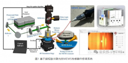
Peking University develops vibration characteristics etching control equipment for MEMS sensors based on ultra-short pulse laser​


Recently, the research team of the School of Integrated Circuits of Peking University, the National Key Laboratory of Micron and Nano Processing Technology, and the Advanced Innovation Center of Integrated Circuits published "Automatic Pico Laser Trimming System" in the "IEEE Transactions on Semiconductor Manufacturing " journal. for Silicon MEMS Resonant Devices based on Image Recognition" article was awarded the journal's 2023 Best Paper Honor Award (1-3 articles/year). The first author of the paper is Liu Yuxian, a 2019 doctoral candidate in the School of Integrated Circuits, Peking University (supervisor: Professor Zhang Dacheng). The corresponding author is Senior Engineer Cui Jian of Peking University. The co-authors include Professor Zhang Dacheng and Senior Engineer Zhao Qianchengzheng.

Silicon micromachined sensor (MEMS) chips have remarkable characteristics such as small size, low cost, strong environmental adaptability, and easy mass manufacturing. They have become key core devices in important industries such as aerospace, communication electronics, and automotive electronics. The relative error of the MEMS chip microstructure process is large, which brings about asymmetry in its mechanical characteristic parameters, causing the accuracy of the MEMS sensor to degrade and affecting the batch production yield. Currently, the industry still lacks complete error analysis and wafer-level control solutions that are universal, intelligent, and efficient, which has become an industry 'pain point' that needs to be solved in the field of high-end MEMS sensor devices.

In response to the above problems and needs, the Peking University research team carried out the research and development of silicon micro-sensor vibration characteristics etching control equipment based on ultra-short pulse laser, and completed an ultra-short pulse laser light source system, laser optical path system, and three-dimensional precision mobile platform system. , design, debugging and verification of hardware and software algorithms such as CCD image recognition system, sensitive structural mechanical characteristic parameter online identification system and processing residue processing system.

1707834580633.png

Please, Log in or Register to view URLs content!
 

tokenanalyst

Brigadier
Registered Member

Fourier-attention network: A deep neural network for lithographic misalignment sensing​

  • Frequency-domain feature enhancement and a spatial attention mechanism are employed to enhance the accuracy of misalignment sensing.​
  • The proposed Fourier-attention neural network achieves a two-dimensional misalignment sensing accuracy of 0.23 nm at a frequency of 20 Hz.​
  • The experimental results of the proposed strategy illustrate its robustness to both system errors and noise.​

Abstract​

A recurring challenge in integrated lithography is subnanoscale misalignment sensing. In widely-used moiré-based misalignment sensing schemes, measurement accuracy is restricted by the performance of the image processing schemes. This is also a fundamental problem in the field of Fourier optics that has received extensive attention in the science and engineering fields. This paper proposes a Fourier-attention neural network that can achieve real time-lapse misalignment sensing with an accuracy of 0.23 nm. This is enabled by the system's robustness to system errors and noise. We hope that this strategy can provide an effective solution for various misalignment sensing applications and that the approach can be applied to future problems.

Please, Log in or Register to view URLs content!
 

tokenanalyst

Brigadier
Registered Member

A study of diffraction-based overlay (DBO) on a 3nm CFET metal layer​


Abstract
Two of most important parameters for the integrated circuit manufacturing are linewidth and overlay. The linewidth uniformity is guaranteed by good exposure tooling, photoresist material, photomasks, Optical Proximity Correction (OPC), optimized patterning process, and good metrology. The linewidth metrology utilized the Scanning Electron Microscope (SEM) directly, which accuracy is entirely determined by the equipment. The overlay metrology quality, however, not only depends on the equipment performance, but can also depend on the substrate quality. There are two types of overlay measurement techniques, i.e., the Image Based Overlay (IBO) and the Diffraction Based Overlay (DBO). In this paper, we will focus our study on a 3 nm Complementary FET (CFET) metal layer overlay. The dimensions of a 3 nm logic design can be as small as 20~24 nm for the Fin Pitch (FP) and 36~48 nm for the Contacted Poly Pitch (CPP) and a On Product Overlay (OPO) of 2.5 nm is required. We will report our study on the DBO for the metal to metal overlay under typical 3 nm logic CFET design rules and a proposed film stack.

Please, Log in or Register to view URLs content!
 

BoraTas

Captain
Registered Member
This is quite interesting info. Thanks.

Just for reference
Please, Log in or Register to view URLs content!
, while HBM3 is used by NVIDIA H100, memory bandwidth is double.

First HBM2E chip came out in 2019, while HBM3 in 2022.

For Huawei getting HBM3 chips can be a problem, but currently US has still not banned HBM memory for export to China, so Alibaba, Tencent, China Mobile, etc can stockpile HBM3 memory and then provide (not sell) them to Huawei to mount on the Ascend boards for their own use. These AI boards are customized for data centers and are not for general public, each customer get its own board eventually providing its own components.

SK Hynix
Please, Log in or Register to view URLs content!
recently that HBM memory demand is huge...maybe not only due to Nvidia:


I would expect HBM3 stockpiling is ongoing now in China....US can close this loophole at any time, applying some pressure on Korean government, so better buy now while waiting for CXMT.


Maybe this requires a new design....Cerberas can tolerate not working transistors because they have designed in the needed redundancy / isolation of defected cores. New Ascend chip version, designed for SMIC process (not TSMC as the old one), can somehow improve robustness to defects and so increasing effective yield, i.e. the number of working chips per wafer although with less cores and/or limited frequency...
HBM2E is also used by the H100 PCIe version. HBM2E emerged with 1y process. There is HBM2E with 1z and 1-alpha too. If they are at 1z, they should reach 1-alpha within 2 years. Then they can do really good HBM2E or HBM3.
 

gelgoog

Brigadier
Registered Member
I do not get it. Isn't the difference between HBM2E and HBM3 about the I/O?
The process just basically influences memory density and hence price. But I doubt CXMT would have much competition in the HBM market. At least not in China they wouldn't. So price would be a small factor.

The fact that HBM is also basically a stacked memory type might mean someone like YMTC could also try to tackle that. At least they have experience with stacking for VNAND. Xtacking uses wafer bonding with TSV.
 
Last edited:

tokenanalyst

Brigadier
Registered Member

Fourier-attention network: A deep neural network for lithographic misalignment sensing​

  • Frequency-domain feature enhancement and a spatial attention mechanism are employed to enhance the accuracy of misalignment sensing.​
  • The proposed Fourier-attention neural network achieves a two-dimensional misalignment sensing accuracy of 0.23 nm at a frequency of 20 Hz.​
  • The experimental results of the proposed strategy illustrate its robustness to both system errors and noise.​

Abstract​

A recurring challenge in integrated lithography is subnanoscale misalignment sensing. In widely-used moiré-based misalignment sensing schemes, measurement accuracy is restricted by the performance of the image processing schemes. This is also a fundamental problem in the field of Fourier optics that has received extensive attention in the science and engineering fields. This paper proposes a Fourier-attention neural network that can achieve real time-lapse misalignment sensing with an accuracy of 0.23 nm. This is enabled by the system's robustness to system errors and noise. We hope that this strategy can provide an effective solution for various misalignment sensing applications and that the approach can be applied to future problems.

Please, Log in or Register to view URLs content!
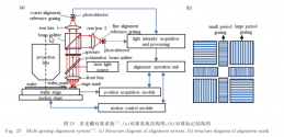
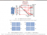
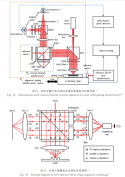
There has been significant development in very accurate sensing technology in China in the last decade:

SMEE 2009:


1707841351342.png

Institute of Optics:
1707841495256.png
10nm.

Harbin Institute of technology 2015:

12nm

SIOM (2017):

2nm

SIOM (2018)

0.13nm

IMECAS (2019):

1707841873184.png

0.05nm

Sensing is everything in lithography, without accuarate sensors it doesnt matter how many billion line of code you have or how fancy your wafer stage is or how powerful of your light source is. Without highly accurate and fast sensors you are not going to pattern any wafers.

Please, Log in or Register to view URLs content!

Looks like China sensing technology has reached subnanometer accuracy.
 
Last edited:

tphuang

Lieutenant General
Staff member
Super Moderator
VIP Professional
Registered Member
Screen Shot 2024-02-13 at 11.36.40 AM.png

Again, I took notes from Q4 earnings call.

Not as interesting as the Q2 earnings, which really just drove home the point that supply chain is changing and domestic suppliers are picking SMIC

market is shifting upward to 28-55nm segment

huge capex and depreciation is interesting, since they continue to invest in outsized fashion for a foundry of their size

They want to add 40-50k 12-inch wafer capacity per year (about 100k 8-inch), but are actually spending enough capex for 100k 12-inch of 28 to 90nm (see their Jincheng & Tianjin plant both budgeted 7.5B capex for 100k).

So basically, a large % of their capex is going into 7nm production. I think $4-5B going into Finfet production.

Which is huge for NAURA, AMEC and other domestic.

Quite interesting since they already bought all the ASML machines they need for a few years. I think 50k wpm of 7nm in 2 years is reasonable estimate. and you can do your own calculation on what that means for the market.
 

AndrewS

Brigadier
Registered Member
Quite interesting since they already bought all the ASML machines they need for a few years. I think 50k wpm of 7nm in 2 years is reasonable estimate. and you can do your own calculation on what that means for the market.

If I do a napkin calculation, 50K wpm @ 7nm might only be enough for all of Huawei's AI and smartphone chips.

And if Ascend 920 are being sold for like 8x their production cost, it certainly makes sense to make as many as possible.
Even the ones with a non-functional core(s) can still be sold for a huge profit.
 
Top