Chinese semiconductor thread II

tonyget

Senior Member
Registered Member
Please, Log in or Register to view URLs content!

ASML CEO Christophe Fouquet: U.S. EUV Export Ban Causes China’s Chip-Making to Lag by 10-15 Years

According to Liberty Times, ASML President and CEO Christophe Fouquet discussed geopolitical issues in the semiconductor industry and China lagging behind the West in chip manufacturing during an interview with the Dutch media outlet NRC.

Regarding the U.S.’s ongoing restrictions on China’s semiconductor development, including the export ban on EUV lithography machines, Fouquet stated that prohibiting the export of these machines to China would cause the country’s semiconductor industry to lag 10 to 15 years. He noted that the ban is indeed effective, according to the report.

However, Fouquet stated that while the U.S. believes ASML should stop servicing and repairing machines in China, ASML takes a different stance. He explained that to prevent Chinese companies from independently maintaining the machines and potentially leaking sensitive information, ASML would like to keep control by continuing to service its machines in China.

When asked about the growing dominance of TSMC and the risks of relying on a single company, Fouquet argued that having only a few major players in the industry could actually foster innovation, as highlighted in the report.

He also expressed confidence in Samsung’s turnover. Regarding Intel, the report noted that Fouquet remarked on the industry’s hope for the company’s revival but cautioned that its future could face significant challenges if mistakes persist. Nevertheless, he underscored Intel’s strategic importance to the U.S., highlighting its critical role in sustaining domestic production of advanced chips for the U.S., as noted by the report.

As for whether the U.S. has underestimated the effort required to develop semiconductor technology, Fouquet pointed out that this is not unique to the U.S.—many underestimate what it takes to build a successful semiconductor company. According to the report, he explained that building a successful semiconductor company demands more than financial investment; it requires significant R&D and years of relentless effort.
 

tokenanalyst

Brigadier
Registered Member

Jishengwei completed the A round of hundreds of millions of yuan, with Shenzhen Capital Group, SMIC Capital and other investors​


According to Huaxin Capital, Jishengwei (Shanghai) Semiconductor Technology Co., Ltd. (hereinafter referred to as Jishengwei) has completed its Series A financing. Guangdong Jin Fund, Shenzhen Capital Group, Shuimu Venture Capital, Shengshi Investment, Wuxi Venture Capital, Zhongxin Juyuan Investment, Shengjing Jiacheng Fund, Dongyuan Venture Capital, Dinghang Capital, Hengqin Danhe Capital, Ningbo Jinkong, Kunpeng Yichuang and other 12 companies jointly invested. The company now has quartz, silicon, vacuum pump, and silicon carbide parts business, and will continue to incubate parts and materials in other segments to create a leading domestic platform-type semiconductor parts company.

Jishengwei was founded in 2021, focusing on the localization of key semiconductor components and services, and striving to become a first-class semiconductor manufacturing comprehensive solution provider. Headquartered in Shanghai, it has R&D centers and manufacturing bases in Shaoxing, Ningbo, Wuhan, etc., with more than 270 employees. Jishengwei actively seizes the opportunity of domestic substitution of key semiconductor components and materials, and has laid out quartz components, silicon components, silicon carbide materials and components, vacuum pump maintenance and other businesses.

According to Huaxin Capital, Ji Shengwei has hundreds of advanced production equipment and has core precision manufacturing process technologies that meet the production environment of integrated circuit-level components. It has stable mass production and supply capabilities and has successfully developed a number of key bottleneck components. It has more than 100 product types, which are widely used in process modules such as epitaxy, diffusion, heat treatment, thin film deposition, etching, and cleaning. It serves major domestic integrated circuit manufacturers, silicon wafer manufacturers, and equipment development companies, and has formed mass delivery, quality control, and service capabilities.

Please, Log in or Register to view URLs content!
 

spaceship9876

New Member
Registered Member
in ASML's investor presentation day last month there is info about the NXT:2150i, NXT:2000Ei, NXT:870B and XT:260 starting to ship this year:
Please, Log in or Register to view URLs content!


although china won't be able to buy nxt:2150i or NXT:2000Ei, they could probably buy the NXT:870B and XT:260.
 

tokenanalyst

Brigadier
Registered Member
in ASML's investor presentation day last month there is info about the NXT:2150i, NXT:870B and XT:260 starting to ship this year:
Please, Log in or Register to view URLs content!


although china won't be able to buy nxt:2150i they could probably buy the other 2.
The NXT:870B and NXT:260 are KrF and I-Line dry scanners, China would be better with their own dry scanners rather than buying then from ASML. In fact, I think ASML and Nikon should be banned from selling dry scanners once China can mass produce them, these companies should restricted to selling immersion and EUV only in China.
 

spaceship9876

New Member
Registered Member
The NXT:870B and NXT:260 are KrF and I-Line dry scanners, China would be better with their own dry scanners rather than buying then from ASML. In fact, I think ASML and Nikon should be banned from selling dry scanners once China can mass produce them, these companies should restricted to selling immersion and EUV only in China.
the overlay accuracy and wafers per hour of these new asml machines will likely be much better than china's. china could do with 1 of each to reverse engineer.
 

sunnymaxi

Major
Registered Member
the overlay accuracy and wafers per hour of these new asml machines will likely be much better than china's. china could do with 1 of each to reverse engineer.
seems like you didn't read this thread properly..

dry DUV machine is already in full scale production and good as ASML dry scanners.. Chinese ministry has announced too. so there is no need to buy and i don't think so you can reverse engineer core components. at the end you have to manufacturer.
 

tokenanalyst

Brigadier
Registered Member
the overlay accuracy and wafers per hour of these new asml machines will likely be much better than china's. china could do with 1 of each to reverse engineer.
Doesn't matter, from an operating POV without the immersion scanner those news machines are basically useless and from a reverse engineering POV older litho scanning technology upgrades almost do not bring anything new to the table except some sensor updates and software updates, maybe a new FPGA board and a lot things that will be difficult to import because are parts exclusive to ASML.
 

tokenanalyst

Brigadier
Registered Member

EDA tool supplier Huaxinsheng completes strategic investment of tens of millions of yuan​


According to the Nanjing Venture Capital Group, Shenzhen Huaxinsheng Software Technology Co., Ltd. (hereinafter referred to as "Huaxinsheng") recently announced the completion of a strategic round of financing of tens of millions of yuan. This round of financing was led by the listed company Guangliwei, and jointly invested by Jiangxi Financial Holdings and Xiangjiang State Investment. The funds will be mainly used for product development iteration and market expansion.

Founded in November 2020 and located in Longhua District, Shenzhen, Huaxinsheng is a core supplier of domestic EDA tools, focusing on the research and development and sales of electronic design automation (EDA) for chip architecture design and chip packaging and testing design tools, and is committed to providing stable and efficient solutions for the entire process of system-on-chip (SoC) from design to packaging and testing. Huaxinsheng focuses on the key links of high-end chip design, with the goal of breaking the monopoly of overseas giants and promoting domestic substitution of EDA. It uses the team's strong technical strength and rich project engineering experience, insists on independent research and development, and provides Chinese solutions for chip design EDA. Some of its point tools have been initially commercialized, filling the gap in domestic EDA in this segment, and related tools have been commercially introduced in many leading domestic companies.

Please, Log in or Register to view URLs content!
 

tokenanalyst

Brigadier
Registered Member

Huahai Qingke's independently developed cleaning equipment has been used in batches for wafer regeneration production​


Huahai Qingke stated on the investor interaction platform that the company's CMP equipment includes a cleaning module, and the cleaning technology is independently developed by the company. Based on the company's technical accumulation in this field and the needs of integrated circuit customers, the company actively carries out the research and development of cleaning equipment, mainly for the terminal cleaning market demand on the material side. The cleaning equipment independently developed by the company has been used in batches for the company's wafer regeneration production. The brush cleaning equipment used for 4/6/8-inch compound semiconductors and the 12-inch single-chip terminal cleaning machine have achieved the first acceptance, and the cleaning products are progressing smoothly.
1735048335740.png
Previously, Huahai Qingke stated in an institutional survey that in recent years, the company's product performance indicators and reliability have been highly recognized by customers, and its market share has increased year by year. This year, new orders have been full, and orders for CMP equipment, wafer regeneration, etc. have all seen good growth. The thinning equipment has obtained batch demo orders from leading companies in many fields, and the company has sufficient orders on hand.

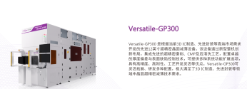
Huahai Qingke also actively seizes the development opportunities in advanced packaging fields such as Chiplet and HBM, comprehensively deploys thinning equipment, dicing equipment, edge polishing equipment, etc., and continues to promote the research and development and verification of related equipment. The 12-inch ultra-precision wafer thinning machine Versatile-GP300 has passed acceptance in the third quarter; 12-inch wafer edge cutting equipment that meets the manufacturing processes of integrated circuits and advanced packaging has been sent to many customers for verification. With the development of the domestic advanced packaging market, the market demand for thinning-related equipment will be greatly increased, which will help consolidate and enhance the company's core competitiveness.

Please, Log in or Register to view URLs content!
 

tokenanalyst

Brigadier
Registered Member

Jiaocheng Ultrasound Headquarters Base and Advanced Ultrasound Equipment Industrialization Project was successfully held.​


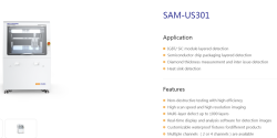
On December 21, the groundbreaking ceremony for the headquarters base and advanced ultrasonic equipment industrialization project of Shanghai Jiaocheng Ultrasonic Technology Co., Ltd. (hereinafter referred to as "Jiaocheng Ultrasonic") was held. The construction project includes the Jiaocheng Ultrasonic headquarters, R&D center, sales center, industrialization center, etc. After the completion of the project, it will give full play to the company's technological advantages and industry leadership, drive the innovative development of the acoustic industry, lead the acoustic-related industries to gather in the "Big Zero Bay" area, help the healthy and sustainable development of downstream application industries, and enhance the company's market share and brand influence.

Semiconductor Ultrasonic Scanning Microscopes
1735049166346.png
1735049200207.png

The project is located in the "Big Zero Bay" science and technology innovation source functional area, and is also in the Jianchuan Road business district of Zhangjiang Minhang Park. The project's goal and positioning is to rely on the regional advantages of the "Big Zero Bay" and take the technical advantages and innovation platform of Jiaocheng Ultrasound as the engine to build the Jiaocheng Ultrasound Headquarters Base and the advanced ultrasonic equipment industrialization project to form an innovation highland for the southern Shanghai Science and Technology Innovation Center, give full play to the leading advantages of Jiaocheng Ultrasound Industry and the regional advantages of "Big Zero Bay", and take the lead in creating a riverside sound valley belt to lead the gathering of acoustic-related industries; deepen the vertical integration of production, education, research and application, and apply ultrasonic technology to semiconductors, wiring harnesses, tire cutting, fuel cells, medical and aesthetic medicine, rail transit, communications, aerospace and other fields, improve the multi-chain reconstruction of the innovation chain, industrial chain and value chain, promote the high-quality development of Minhang's economy, create a Shanghai science and technology innovation brand, and support the implementation of national strategies.

Please, Log in or Register to view URLs content!
 
Top