Chinese semiconductor thread II

tokenanalyst

Brigadier
Registered Member

Huawei will launch Vision head display: self-developed chip, 350 grams, about 15,000 yuan​

Li Nan, former CMO of Meizu Technology and now founder of Numiao Technology, recently posted on Weibo, claiming that Huawei is developing a Vision headset, priced at around 15,000 yuan.

It is reported that this headset will use Huawei's self-developed chip, with "almost no delay" in spatial operation, and will be equipped with a Sony 4K Micro-OLED screen (the relevant screen is expected to be shipped within a month). It weighs 350 grams, which is 350 grams compared to Apple. The Vision Pro headset has removed the "eyesight" feature.
Previously, media reported that Huawei had launched a Vision Glass head-mounted display (smart viewing glasses) in 2021. The glasses are equipped with dual 1080P Micro-OLED screens and are mainly used for viewing.
MBXY-CR-982e4258353ebd898fd3da95b29d440c.png

▲ VR Glass previously launched by Huawei
According to previous reports, Huawei registered the "Vision Pro" trademark in 2019. The trademark belongs to International Classification 9 and covers a variety of goods and services such as LCD TVs, head-mounted virtual reality devices, and radio equipment. In addition to Vision Glass In addition, Huawei also uses the relevant Vision trademark on the Vision smart screen, so Apple Vision Pro may use another name when it is launched in China.​

Please, Log in or Register to view URLs content!
 

tokenanalyst

Brigadier
Registered Member

Novel CPU cache architecture based on two-dimensional MTJ device with ferromagnetic Fe3GeTe2​


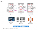
With the development of Artificial Intelligence (AI) in recent years, the fields of computer, biology, medicine, and aerospace have demanded higher requirements for the processing and storage of information. In this paper, a novel Magnetic Tunnel Junction (MTJ) based Spin-Orbital Torque Magnetic Random Access Memory (SOT-MRAM) composed of Fe3GeTe2 (FGT) is employed as a storage medium in the computer architecture. On the basis of the analysis of the fundamentals, model configuration, characteristics and performance advantages of the FGT based SOT device, a hybrid storage (L1, L2, Last Level Cache) is constructed, with FGT-SOT-MRAM, conventional SOT-MRAM and STT-MRAM replacing the original static random access memory (SRAM) in the novel triple-level CPU cache architecture. This can override the increasing leakage problem of SRAM, while opening up the application of two-dimensional van der Waals ferromagnets in computer systems at the L1 cache level. Meanwhile, an innovative cache optimization scheme is put forward for magnetic memory to better match the performance of FGT-SOT-MRAM to CPU. The simulation results demonstrate that the FGT-based MRAM can achieve up to 38.03% IPC optimization and 53.41% power optimization in the CPU cache system in contrast to the conventional ones.

View attachment 125133View attachment 125134
View attachment 125135

Please, Log in or Register to view URLs content!

More

Advanced hybrid MRAM based novel GPU cache system for graphic processing with high efficiency​


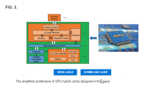
With the rapid development of portable computing devices and users’ demand for high-quality graphics rendering, embedded Graphics Processing Units (GPU) systems for graphics processing are increasingly turning into a key component of computer architecture to enhance computability. The cache system based on traditional static random access memory (SRAM) plays a crucial role in GPUs. But high leakage, low lifetime and poor integration problems deeply plague the science and engineering field. In the paper, a novel magnetic random access memory (MRAM) based cache architecture of GPU systems is proposed for highly efficient graphics processing and computing accelerating, with the merits of high speed, long endurance, strong interference resistance, and ultra-low power consumption. Spin transfer torque-MRAM and spin orbit torque-MRAM are utilized in off-chip and on-chip caches, respectively. A controller design scheme with prefetching modules and optimized cache coherency protocols are adopted. After testing and evaluating with multiple loads, neural network models and datasets, the simulation results show that the proposed system can achieve up to 28%, 56%, and 66.45% optimizations mostly in terms of speed, energy and leakage power, respectively.

1707575701268.png1707575745832.png
1707575783688.png

Please, Log in or Register to view URLs content!
 

tokenanalyst

Brigadier
Registered Member

Biren Technology and AsiaInfo Data signed a strategic cooperation agreement​


Recently, Biren Technology and AsiaInfo Data officially signed a strategic cooperation agreement. The two parties will rely on Biren Technology's technical strength in general-purpose GPU software and hardware systems, give full play to AsiaInfo Data's deep industry accumulation in large model algorithm applications, accelerate the application of domestic computing power products, and jointly promote the continued vigorous development of China's artificial intelligence industry.

As China's computing power infrastructure construction enters an explosive period, building a mature ecosystem around domestic computing power has become the top priority for industrial development. Biren Technology and AsiaInfo Data will carry out close cooperation in the construction of computing infrastructure, construction of computing platforms, implementation of domestic general-purpose GPU applications, and research on major issues to promote the construction of industrial ecology.

Please, Log in or Register to view URLs content!
 

tokenanalyst

Brigadier
Registered Member
Not everyone who works for think tanks says bullshit due to their lack of knowledge. Some of them simply do it for money because they are paid to create a certain narrative and opinion among the public. The way he post things, very much sound like someone who would work for such a think tank.
He had an account here for several years but didn't post anything. Then first time he posted he started asking questions like How many 28nm machines have SMEE shipped? Are they being used in SMIC/YMTC? Which cities Huawei constructing their fabs? He said he was doing research for investing in semi companies. Then few days later he claimed to have insider knowledge more than anyone else, which would make those questions pointless. If someone posts expert information here and the others are convinced that he is an insider, the other insiders are more likely to share information with them that they would not share in the public.
I don't know if he is really hvpc but reading through the posts it think it looks like that this person or either work at BIS or is really close to and advice the others D.C. think tankers. Something suddenly really trigger him, this lasts post about SMEE are pretty salty and bombastic, he even dismissed Dylan Patel in one his post and we know that Dylan is pretty much not a fan anything related to China semiconductor industry. All that after SMEE updated their website. My hypothesis is that there is A LOT of drama between the Semiconductor industry and the think tankers in D.C. related to the consequences of these export controls, the writing is pretty much in the wall, lot of angry calls and shouting from the Netherlands and Japan industry leaders. Another thing is that twitter sucks even more now.​
 

BoraTas

Captain
Registered Member
More

Advanced hybrid MRAM based novel GPU cache system for graphic processing with high efficiency​


With the rapid development of portable computing devices and users’ demand for high-quality graphics rendering, embedded Graphics Processing Units (GPU) systems for graphics processing are increasingly turning into a key component of computer architecture to enhance computability. The cache system based on traditional static random access memory (SRAM) plays a crucial role in GPUs. But high leakage, low lifetime and poor integration problems deeply plague the science and engineering field. In the paper, a novel magnetic random access memory (MRAM) based cache architecture of GPU systems is proposed for highly efficient graphics processing and computing accelerating, with the merits of high speed, long endurance, strong interference resistance, and ultra-low power consumption. Spin transfer torque-MRAM and spin orbit torque-MRAM are utilized in off-chip and on-chip caches, respectively. A controller design scheme with prefetching modules and optimized cache coherency protocols are adopted. After testing and evaluating with multiple loads, neural network models and datasets, the simulation results show that the proposed system can achieve up to 28%, 56%, and 66.45% optimizations mostly in terms of speed, energy and leakage power, respectively.

View attachment 125137View attachment 125138
View attachment 125140

Please, Log in or Register to view URLs content!
Most of the research on non-conventional storage devices dates to the early-2000s era when there was a research on flash memory. NAND won that contest.

The current research is being triggered by multitude of factors like:
- ML requiring a lot of computing power
- Relative plateau in chip performance, especially regarding per USD and Watt performance
- ML being heavily dependent data handling performance and not requiring precise calculation.

SRAM is much faster than MRAM but, in a data intensive application like ML, it might be better to have more data on the die (or least in the same package) rather than faster storage.

Not gonna lie it is an interesting proposition, especially for me as I work on things related to processor caches daily. Nice to see it is being researched. I don't think MRAMs will be used in general purpose processors though. Cache performance is the single biggest constraint of processor speed in most applications.
 

tokenanalyst

Brigadier
Registered Member
Make the machine bigger or shorten the wavelength

Enhancement of 6.7 nm EUV emission from laser-produced Gd plasma with micro-structured target​

Abstract​

We present the experimental investigations of extreme ultraviolet (EUV) radiation of laser-produced plasma based on the micro-structured Gd target and obtain a strong EUV radiation intensity at the wavelength of 6.7 nm. The intensive extreme ultraviolet radiation and narrow-band spectra are achieved by laser irradiation in the groove position of the target. The spectral widths from the micro-structured target are approximately two-thirds width of that of the flat target, and the EUV intensity enhancement ratio is 1.48 comparing with that of the flat case. The measurements of the electron density of Gd plasma were performed using Nomarski interferometry. The results show that the plasma generated by the micro-structured Gd target is confined by the groove between the micro-columns. The plasma electron density distribution is mainly concentrated in the laser incidence direction and the density is higher than that of planar target. Finally, the parameters of the groove width of structured target and laser energy are varied to enhance the EUV radiation. This study shows that the confinement effect of the structured target can improve the extreme ultraviolet radiation. Those findings are expected to provide new approaches in developing the next-generation extreme ultraviolet light source.

According to the Quasi-Moseley law [6], the n = 4-n = 4 transitions from Gd12+∼Gd25+ yield intense unresolved transition array (UTA) that emits radiation concentrated at wavelength of 6.7 nm. Moreover, the recent studies have shown that LaN/B4C multilayer mirrors (MLM) exhibit a remarkable reflectivity of up to 57 % at 6.7 nm [7,8]. This indicates that laser-produced Gd plasma could be a promising candidate as next generation extreme ultraviolet light source.

Please, Log in or Register to view URLs content!
 

tokenanalyst

Brigadier
Registered Member
1707667351225.png
2.1 Experimental setup The schematic view of the experimental equipment and computational model is depicted in Figure 1. The traditional parallel plate CCP discharge system was optimized for MLM self-discharge cleaning [6]. This system was utilized to simulate the MLM discharge, where the electrode (30 mm) is regarded as a substitute for MLM, and the external grounding ring was used to generate plasma with the electrode and constrain the range of plasma generation. An ICP cleaning device was utilized to compare the effect of plasma cleaning with atomic hydrogen cleaning, see Figure 1(b). Two layers of 150 mesh molybdenum mesh were installed below the quartz tube to filter out hydrogen ions, allowing only hydrogen atoms to pass through. The background vacuum of the device is 10-4 Pa. The experimental setups included a 13.56 MHz plasma source, an RF compensation Langmuir probe, a deceleration field ion energy analyzer (Impedans, Semion), and a sheathed thermocouple. Detection equipment was used to diagnose plasma parameters and electrode surface temperature. The Quartz Crystal Monitor (QCM, Inficon, SQM-160) was the tool to measure thin film thickness. The thickness of redeposition during plasma cleaning was in-situ monitored through QCM. Contamination samples of 1 cm 1 cm were prepared by physical vapor deposition(on silicon wafers) [6]. Not dense and nonuniform tin particle contaminations were prepared for studying the cleaning process.

4. Conclusion
This work adopted the electrode structure based on CCP discharge mode to simulate MLM selfdischarge. The electron density (~1015 m-3), electron temperature (~5 eV), and hydrogen radical distribution (~1017 m-3) on the electrode surface were simulated using the plasma module in COMSOL software at 1 W. The ion energy distribution function on the electrode surface was obtained by employing a charged particle tracking module in COMSOL, and the accuracy of the simulation results was verified through the measured ion energy data in the experiment and the impact of the plasma sheath on ion energy under the electrode bias voltage. The ion energy distribution at the electrode surface was 23-40 eV and mainly concentrated at 32 eV. The possibility of tin contamination melting was determined by calculating the energy transfer caused by particle collisions, and this result was confirmed by comparing the evolution of tin particle morphology after plasma cleaning (spherical to conical) and annealing. By comparing and analyzing the effects of hydrogen atom cleaning and plasma cleaning on the morphology of tin particles, it was discovered that the influence of hydrogen atoms did not lead to the morphological evolution of tin particles. The effect of redeposition on the evolution of tin particle morphology was excluded after monitoring the redeposition rate (0.00108 Å/s) during plasma cleaning. Combining this study with previous studies, ions play two leading roles in cleaning. Firstly, ions break the Sn-Sn bonds to provide binding sites for hydrogen atoms. Secondly, in the initial cleaning stage, the melting deformation of tin particle contaminations under the ion thermal effect increases the interaction area with hydrogen atoms, thereby increasing the cleaning rate.

Please, Log in or Register to view URLs content!
 

gadgetcool5

Senior Member
Registered Member
I think he is mostly memeing because hvpc is one of the more week known individuals here with similar skeptical sentiments, but I think what is a legitimate common trait being implied, is the inability to recognise and track Chinese side semiconductor rumours in a competent manner, and reliance on "official" releases of information as a gauge of actual progress or state.

In that sense, it is less so much that hvpc and this person are similar and more that that type of thinking is the usual way of tracking Chinese semi development by the majority of foreign observers, professional or not.
I hope this is not stepping out of bounds to ask this question, but why should anyone put stock in rumors?

Anyway, he retweets/interacts with people like Dylan Patel and Jordan Schneider. Definitely part of the blob.
 
Last edited:
Top